Powering Processors and FPGAs with the New TDK µPOL
A new ‘plug and play’ solution to power complex ICs can space and design time without compromising performance.
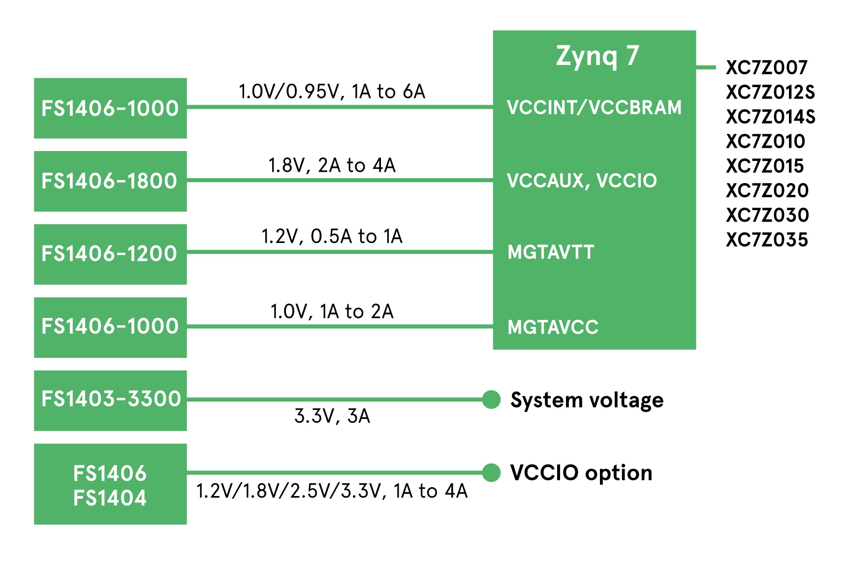
Figure 1: A typical ‘power tree’ for a Xilinx Zynq 7 device
Minimising power consumption is a high priority and in digital devices, it is directly related to voltage swing and data rates. Consequently, supply voltages have steadily reduced from 5V to sub-1V with sub-sections of devices having separate supply rails: processor cores between 0.56V to 0.88V on next generation 7nm technology, a similar voltage for block RAM, 1.35V or 1.5V for DDR memory, 1.5V for auxiliary functions and 3.3V and 5V for legacy I/O. Further SoC integration is adding additional voltage requirements for DSP, codecs and video/graphics processing and often multiple, similar voltages need to be generated separately, to avoid interactions, and so they can be individually enabled and power sequenced.
Low voltages mean high currents for a given power, with some SoCs, FPGAs and processor cores now drawing more than 200A. Other rails might be from 1A to 25A for memory, SERDES, and I/O voltages. These rails are derived from Point of Load (PoL) regulators from a higher bus voltage, typically 5V or 12V, where the current is much lower for the power drawn. System designers will generate a power ‘tree’ diagram to summarise the arrangement (Figure 1).
Putting PoL converters close to devices like FPGAs poses problems though; a typical FPGA such as in the Xilinx UltraScale range has more than 1000 BGA connections and is surrounded by supporting devices for I/O as well as a substantial heat sink. Space is at a premium and the PoLs have to fit in where they can, especially in small form factor applications such as FPGA SoM cards and PCIe cards. The ideal PoL is therefore highly efficient and small without needing heatsinking, and low profile, so that it can be back-side mounted or even fitted under other components such as board-mounted piggybacks or sub-boards. Of course, it must also provide a precise voltage under static and dynamic load conditions, have output control for shutdown and sequencing and be fully protected against shorts, over- and under-voltages, and over-temperature stress. Modern PoL devices will also have communication features, typically over a I2C bus using PMBus commands, to set up device characteristics, as a one-time adjustment for fault detection thresholds for example, or even ‘on-the-fly’ for dynamic control of output voltage for energy saving. The bus can also signal PoL conditions such as load current, temperature and status.
PoL basics
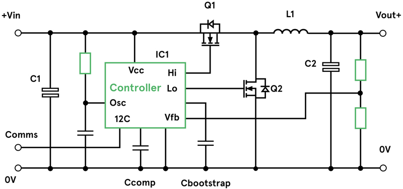
Figure 2 shows a basic PoL converter. Q1 and Q2, switch alternately to supply load current and ‘charge’ inductor L1 in Q1 on-period and discharge its energy through Q2 to the load during Q1 off-period. Controller IC1 samples the output and drives Q1 and Q2 with pulse-width modulated signals to achieve regulation of the output voltage in conjunction with L1 and C2. IC1 also monitors and detects abnormal conditions and integrates the communications function.
Click image to enlarge
Figure 2: PoL basic schematic, single phase type
Component selection is a trade-off; L1, C1 and C2 can be smaller at higher switching frequencies, but this produces more dynamic losses in Q1 and Q2, requiring a bigger part to dissipate the heat. Advances in MOSFET technology, however, allow operation in the MHz range today.
PoL designs - the ‘old’ way
Components in the PoL shown in Figure 2 are discrete and could be placed on the motherboard. However, PoL design is a particular skill and it is very difficult to achieve optimum performance when the PoL is mixed in with other motherboard components, also consuming precious motherboard space.
Modular PoLs have been available, offering the advantage of a single component to source, saving the customer design and qualification overheads, as well as procurement, stocking and placement of multiple discrete components. However, older modules occupied a similar footprint to a discrete solution and were expensive. More recent modules though have integrated the discrete components into smaller packages with some vertical stacking arrangements giving real footprint savings. SIP versions occupy little footprint but are tall and typically require through-hole soldering. Hybrids are also available, comprising just the power components of the PoL with the controller placed separately on the motherboard, perhaps on the back side, giving some space saving. Figure 3 shows components in a typical discrete implementation of a PoL, occupying about 50 mm2 for 6A amp rating. Input and output filtering capacitors are not included and MOSFET switches are integrated in the controller.

Click image to enlarge
Figure 3: A discrete implementation of a 6A PoL converter with necessary peripheral components excluding input/output capacitors
Chip embedded technology – next generation PoLs
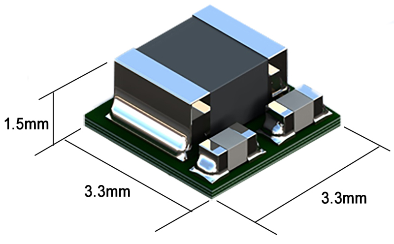
Withmotherboards shrinkingdown to smaller platforms such as in PCIe, CoM boards, SSD, Edge and AI computing, the market demandsmore compact power conversion solutions. To achieve a step improvement, TDK has taken a ‘clean whiteboard’ approach with the design of its new µPOL range of modular PoLs, for 5W to 150W systems (Figure 4). Proprietary, patented technologies have been combined to yield a dramatic improvement in footprint and current density. The FS140x series, initially available in 3A, 4A and 6A versions will be expanded in the future to 25A and on to 100A. The products available now are in a tiny 3.3mm x 3.3mm package just 1.5mm tall for placement in height-constrained areas such as on the backside of the motherboard or under other components such as heatsinks and daughter boards. Power density achieved is a class-leading 1W/mm3 – 15 watts in a 3.3mm x 3.3mm space without airflow cooling. Like competing PoLs, external input and output capacitors need to be added for a full implementation but these are small due to the high switching frequency employed. From a system point of view, it is better to add the capacitors externally, as they can be dimensioned for the exact voltage and load transient response requirements of the application. Otherwise, capacitors would have to be sized for the highest possible load and highest possible input and adjusted output voltage, adding unnecessary cost and board space.
Click image to enlarge
Figure 4: The µPOL from TDK with a footprint of just 11mm2 and 1.5mm height
With the TDK µPOL in a minimal configuration, apart from input/output capacitors, no other components are required such as compensation networks, output setting resistors, bootstrap or pin decoupling capacitors.
Key to the improvements achieved are TDK’s thin film inductor technology and a new technique, SESUB or Semiconductor Embedded in substrate, integrating the MOSFETs and control IC into the layers of a 250µm thick substrate with the inductor placed on top. There are no wire bonds, making the devices very robust, and the parts are light, therefore suitable for drone, machine vision and other small form-factor applications. Thermal characteristics are controlled so that heat from the IC and inductor is effectively led through the substrate terminations to the motherboard. This is so effective that at full 6A output, the module temperature rise is just 41°C (12V input and 1.8V output).
Click image to enlarge
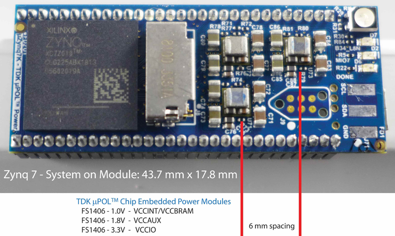
Figure 5: µPOL PoL converters small form-factor FPGA power design
System benefits with the µPOL
The tiny footprint of the µPOL enables the smallest of spaces to be utilised for voltage regulation close to target devices. Output voltage is selectable from 0.4V to 5V and input voltage range is 4.5V to 16V with a single supply and 2.5 to 16V with an extra auxiliary supply providing a bias voltage. Applications are scalable, as the 3A to 6A parts have the same footprint.
Integrated monitoring and control functionality in the µPOL also add significant system benefits: for example, a ‘power good’ output and ‘enable’ input can be utilised for ‘ratiometric’ or ‘simultaneous’ power sequencing of multiple µPOLs. Protection is comprehensive with output over-voltage, input under-voltage and output over-current or short circuit monitored, all with selectable thresholds, with ‘hiccup’ mode shutdown. The devices operate over the range -40°C to +125°C with programmable thermal shutdown and auto-recovery.
The built-in I2C interface supports Fast and Fast Plus modes and enables a wide range of settings via PMBuscommands:
· Settable output voltage, 0.4V to 5V with 5mV resolution (fixed input versions initially available – variant dependent)
· Output voltage trim, (+/- 0.5% initial accuracy)
· Optional soft start and stop rates 0.5mV/µs or 1mV/µs
· Adjustable PGood Threshold: 85%, 90% and 95% of Vout
· Adjustable OVP threshold: 105%, 110%, 115% and 120% of Vout
· Adjustable OVP scheme: Latch, Unlatch
· Adjustable OCP threshold: up to 8A with 250mA resolution
· Adjustable OTP threshold: 75oC, 85oC, 125oC and 145oC
· Selectable ‘continuous’ (CCM) or ‘discontinuous’ (DCM) operating modes for EMI and efficiency optimization
With a wide range of devices, options and settings, system designers can ‘tune’ applications using the µPOL for minimum system cost and maximum functionality.
Application example
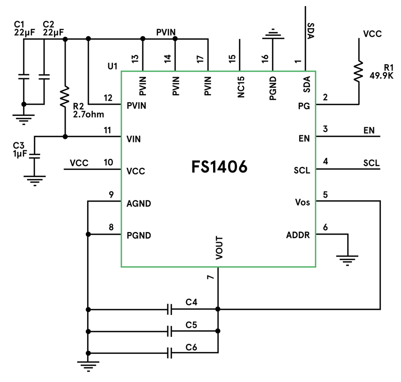
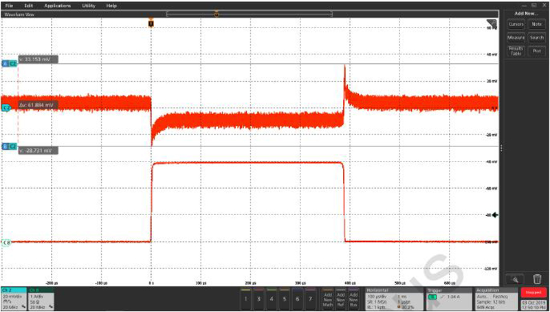
Figure 6 shows the TDK µPOL configured for Vin = 12V, Vout = 1.8V and Iout = 6A with ripple voltage requirement less than +/-1% pp Vout and a maximum Vout excursion of +/-3% with a 3A load step. The µPOL part is FS1406 and 2 x 22µF capacitors are initially chosen for both Cin and Cout. Switching frequency Fsw is 2MHz.
Click image to enlarge
Figure 6: The TDK FS1406 µPOL in a typical application
Input capacitor selection depends on ripple current handling IRMS. In a buck converter operating at duty cycle D, this is given by:
Here, Iout is 6A and D = Vout/Vin = 0.15, giving IRMS= 2.14A which is easily handled by two 22µF, 16V capacitors type TDK C3216X5R1C226M160AB.
The minimum number of output capacitors required, NMIN to meet the target ripple ΔVoutis given by:

TDK MLCC capacitors C2012X5R0J226K125AB have an ESR of 3 milliohms, an ESL of 0.44nH and an effective capacitance of 12µF at 1.8V. Solving, NMIN is 1.27 so 2 capacitors as assumed is adequate.
The minimum number of capacitors to meet the load transient response ΔVoutmax with load step ΔIout is given by:
Solving again with 12µF, NMIN is 0.4 so two TDK capacitors C2012X5R0J226K125AB is a good solution.
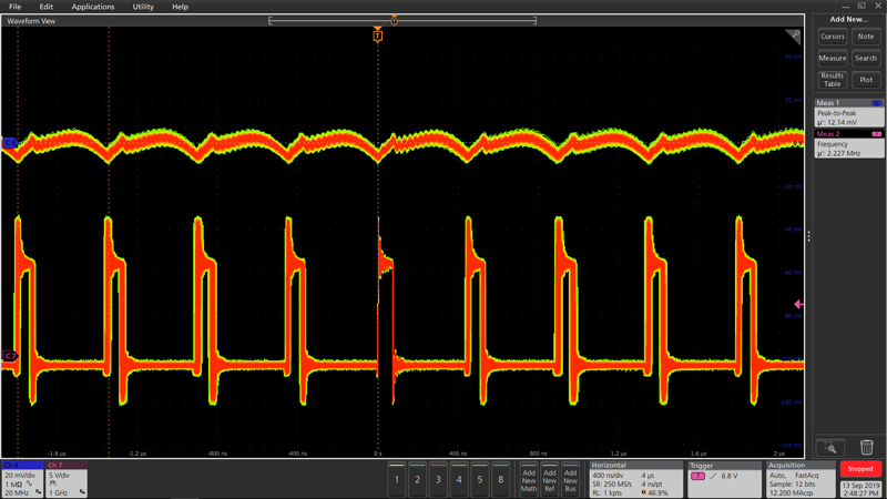
The resultant ripple and load transient response plots are given in Figures 7 and 8 showing just 15.19mV pp ripple or 0.8%, and about 30mV excursion or +/-1.7% with load steps.
At higher output voltages, the minimum number of 22µF output capacitors decreases for the same ripple and transient load specification and above 2.25V output, just one is required.
Click image to enlarge
Figure 7: Ripple, application example, 6A, 1.8V output
Click image to enlarge
Figure 8: Transient load response, +/-1.7% excursion with a 50% load step
TDK µPOL- includes comprehensive support
To support design-in of theµPOLT, TDK provides a suite of tools including general purpose evaluation boards with interfaces to access the I2C bus, with an easy-to-use GUI to set up the parts. Additionally, ‘Power Strip Design Boards’ are also available with up to eight µPOL units fitted to provide all the rails, including sequencing boards, for Xilinx Spartan 7, Artix 7, Zynq 7, Zynq UltraScale+, Zynq UltraScale+ RFSoC, Versal ACAP (Versal Prime Series) and other FPGAs from vendors such as Altera, NXP (i.Mx8, LS series), Marvell/Cavium and Microsemi. For quick implementation, schematics are provided along with PCB ‘layout snippets’ for ORCAD/Allegro, Altium and Mentor PADs+/Xpedition CAD programs. ‘Ready to go’ power subsystem solutions for vendor FPGAs are available from TDK and, as a Xilinx ‘Alliance Program Certified member’, TDK has generated complete reference designs for FPGAs such as the Zynq7 series.


