Presto Engineering Upgrades Europe's Largest Independent Semiconductor Testing Facility to ISO 9001:2015 Standard

Date
10/10/2018

 PDF

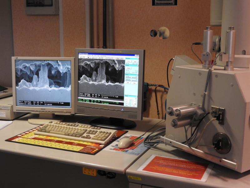
Scanning electron microscope at Presto Engineering.

 
"We have an extensive and comprehensive range of semiconductor test equipment," said Dr Alban Colder, Presto's Site Director at Caen. "This includes testing at every stage from wafer, through die, to final packed device. As part of the ISO 9001: 2015 quality standard, we have a comprehensive range of equipment for non-destructive analysis such as X-Ray to check packaging and bondings, and ultrasound to see inside a device to check for delamination, voids and cracked silicon. There is also equipment to check for failure localization by photoemission or thermal laser stimulation, and deep physical analysis, i.e. strip a device down layer by layer to see exactly where it is failing and why. Other advanced equipment such as an atomic force microscope or a scanning electron microscope are used to reveal the precise details of the structure of a chip down to a few nanometers."
 
 
Martin Kingdon, Presto's VP of Sales, added, "We have assembled a suite of state-of-the-art equipment as part of our commitment of quality and this new standard. We provide customers with a comprehensive service once they provide us with a design that covers every stage of the chip manufacturing and testing process right through to final product. As part of our quality assurance to customers, we rigorously test at every stage. Such a comprehensive test and failure analysis capability all together under one roof is very rare; usually it requires a number of different test houses which means that issues could be missed. Having all the skills and equipment together in one place means that we can keep searching until we find the cause of a problem so that it can be resolved and quality maintained."
 
For more information, visit: www.presto-eng.com.

RELATED


-->