Protect Small Sensors from the Harsh Industrial Environment

Sensors are ubiquitous in the electrically harsh industrial environment
Figure 1. Welding in Automotive Assembly Line
Sensors are ubiquitous in the electrically harsh industrial environment (Figure 1). As they increase in sophistication and shrink in size, they become more complex, requiring on-board switching regulators to deliver power more efficiently for minimal heat generation. How do you safely deliver low-voltage power to tiny sensors in high-voltage, industrial environments, while minimizing solution size and maximizing efficiency? In this design solution, we will review a typical industrial sensor architecture and provide an innovative solution to this challenge.
Safe PowerChallenge
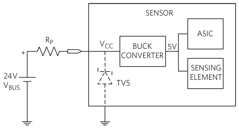
The sensor ”box” includes a front-end transceiver that handles data and routes the power to a step-down buck converter, which delivers the appropriate voltage to the ASIC/microcontroller/FPGA and sensing element. The sensor is typically powered by a 24V DC power source (VBUS). The power path is shown in Figure 2.
Click image to enlarge
Figure 2. Sensor Power System
If the 24V bus is clean or has an electric noise level below the operating voltage of the front-end switching regulator, no protection is necessary (no TVS in Figure 2) and a buck converter with a typical max input voltage of 36V or 42V is sufficient for this sensor design.
However, the factory floor can be a very challenging environment, with long cables and strong electromagnetic interference resulting in high-voltage transients. Accordingly, the step-down converter inside the sensor must withstand voltage transients much higher than the sensor operating voltage.
A typical sensor power management solution utilizes transient voltage suppressors (TVS) to limit the input voltage (VCC) of the front-end buck converter. The associated input current peaks are reduced by the resistor RP, a parasitic or physical element in the electric path between the voltage transient’s source (VBUS) and the sensor.
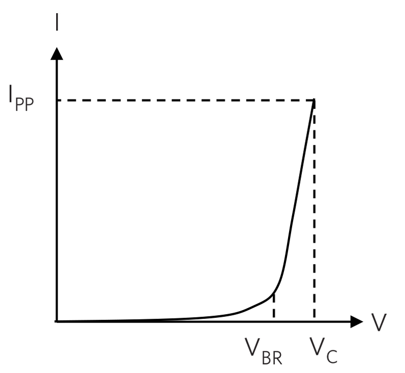
Let’s see how to select a TVS out of the LittelfuseTM catalog as an example. The general characteristics of a TVS are shown in Figure 3.
Click image to enlarge
Figure 3. TVS V-I Characteristics
The TVS device is an open circuit until the voltage across it reaches VBR. At this point, it starts to conduct current while its voltage rises slightly up to its maximum clamping voltage VC, which corresponds to the maximum allowed peak pulse current IPP. The product VC x IPP is the maximum peak power that the TVS can handle (400W for this TVS family).
For effective protection, the TVS VBR must be chosen to be above VCC(MAX) while VC must be below the switching regulator input voltage breakdown.
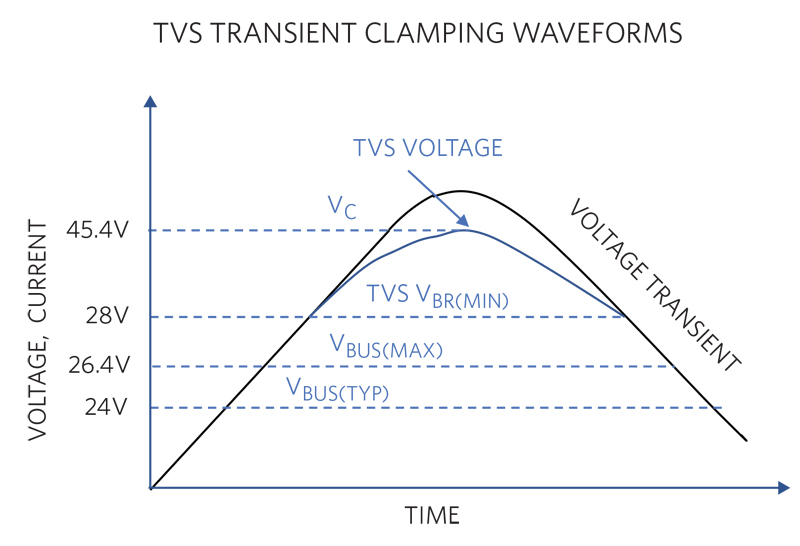
Our VBUS supply is 24V ±10%, with 26.4V maximum (VBUS(MAX)). The closest possible TVS choice from the catalog is the SMAJ28A, with a minimum 28V VBR, a 45.4V maximum clamp voltage and an 8.8A maximum peak current (Figure 4). The delta between the TVS voltage and the voltage transient develops the current through the resistor, RP, which has to be below the maximum allowed IPP.
Click image to enlarge
Figure 4. Minimum TVS Selection
The fact that our buck converter must withstand 24VDC and at least a 45.4V transient removes a large group of buck converters from consideration.
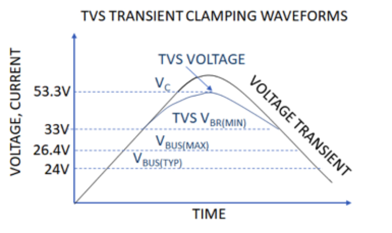
Additionally, with the selection above, there is only a 1.6V margin between the maximum VBUS and the minimum TVS voltage (VBR). A higher margin requires a voltage rating for the buck converter (VCC) well above 45.4V. Ideally, with a 60V-rated buck converter, a SMAJ33A with a minimum VBR of 33V can be used (and a clamp voltage VC of 53.3V, well below 60V). This gives an operating margin of 6.6V above VBUS(MAX) and 6.7V below 60V (Figure 5).
Click image to enlarge
Figure 5. Ideal TVS Selection
Sensor Miniaturization Challenge
For sensor miniaturization, the typical PCB strategy of placing all the buck converter components on the same plane is not ideal. In Figure 6, a 300mA buck converter IC and passives (L,R,C) require a hefty PCB area (29.3mm2 net area).

Click image to enlarge
Figure 6. Typical Planar Buck Implementation (29.3mm2 Net Area)
The Thermal Challenge
Sensors have sealed enclosures (without fans or cooling) due to the harsh environments they sit in. A small amount of heat generated inside this small enclosure can quickly raise the sensor temperature, compromising its reliability. The trend of sensor miniaturization makes their thermal management even more challenging. The solution to the thermal challenge is a buck converter with very high efficiency.
Recalling the above challeges: an efficient buck regulator that fits inside a small PCB area and has a 60V breakdown voltage is necessary to fit inside a small sensor.
The Solution: Vertical Integration
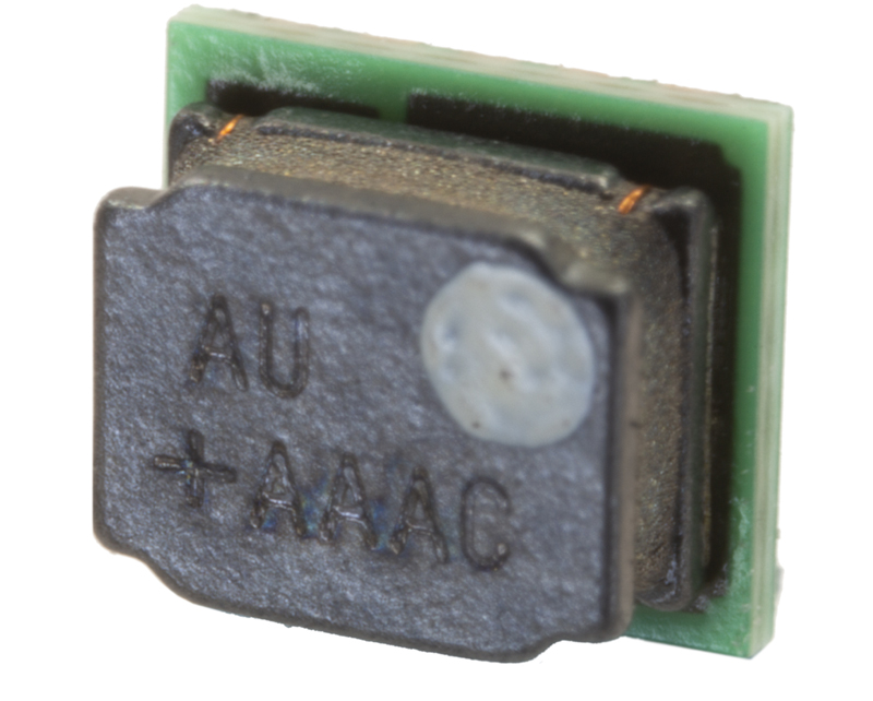
A novel way to solve the space problem is to integrate vertically the inductor on top of the IC. One example is the Himalaya uSLIC™ power module. It delivers more power in a smaller space than ever before, with high efficiency and ease of use. The power module vertically integrates the inductor and the buck converter IC, dramatically reducing the PCB space occupied by the standard buck converter solution. This still meets expectations of high-voltage tolerance and high-temperature operation. The MAXM15064module (Figure 7) is available in a low-profile, compact, 10-pin, 2.6mm x 3mm x 1.5mmpackage. The device operates over a wide temperature range from -40°C to +125°C.
Click image to enlarge
Figure 7. 60V, 300mA module (2.6mm x 3 mm x 1.5mm)
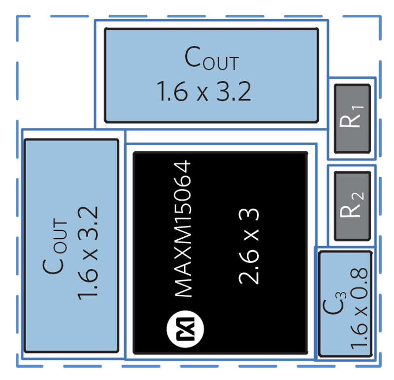
Figure 8 shows the size reduction achieved with the 300mA, 60V buck converter module. The ability to meet a 60V maximum operating voltage (not just absolute maximum rating) and support output voltages below 1.8V. Wtih the vertical integration of the inductor, the net component area is a mere 21mm2.
Compared to the IC solution of Figure 6, the module solution’s net component area is 28% smaller.
Click image to enlarge
Figure 8. 60V, 300mA High-Voltage Module Implementation (21mm2 Net Area)
Minimum Heat Generation
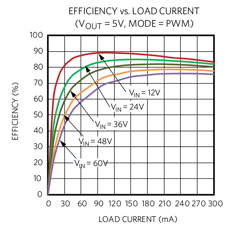
Figure 9 shows the efficiency of the module with 5V output and input voltages from 12V to 60V. Despite the small size, the buck converter delivers high efficiency with peaks up to 90%. For a 24V powered application, the module provides an efficiency well above 80% across most of the operating range, assuring low-power losses and low heat generation.
Clcik image to enlarge
Figure 9. Minimum Heat Generation
Low Emissions
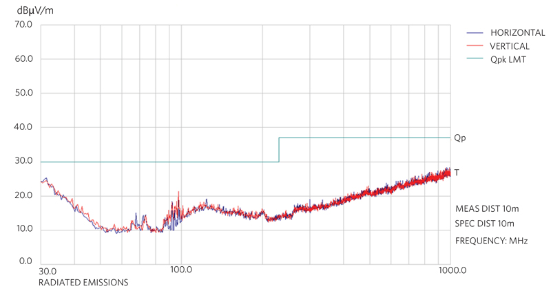
The module’s PCB layout is designed to minimize trace lengths and eliminate ground loops for minimum radiated emissions. The use of high-frequency ceramic capacitors minimizes conducted emissions. Figure 10 shows that the radiated emissions comfortably meet the CISPR22 CLASS B specification.
Click image to enlarge
Figure 10. Radiated Emissions
Figure 11 shows that the conducted emissions also comfortably meet the CISPR22 Class B specification.

Click image to enlarge
Figure 11. Conducted Emissions
Conclusion
We discussed the challenges of safely delivering higher power more efficiently with minimum heat generation for smallindustrial sensor applications. The proper protection of the 24V input power is best served by a buck converter that can withstand a 60V input. Finally, we introduced a disruptive approach that stretches the input voltage rating and the power density envelope with a novel, miniaturized, easy-to-design, high-performancebuck converter module. The power module is a high-efficiency, small-size, low-EMI buck converter ideal forpowering tiny sensors in industrial applications.