Protecting control systems in the field
Differential overvoltage protection circuits for current-sense amplifiers
Harsh environments are a reality for many electrical systems used in motor control or solenoid control applications. The electronics that control motors and solenoids are by necessity in close proximity to the high currents and voltages used to create the physical movement required by the end application.
In addition to proximity, these systems are often serviceable (for example, one might hire a technician to change the controller board for dishwasher solenoid) which leaves open the possibility of unintentional wiring errors. The proximity to high currents and voltage, coupled with a potential for incorrect wiring, necessitate a design that incorporates overvoltage protection.
To create efficient and safe systems, precision current sense amplifiers monitor the currents in these applications. The precision amplifier circuits need to be designed to protect from over voltage conditions, but these protection circuits may impact the accuracy of the amplifier.
With proper circuit design, analysis and verification, it is possible to balance the trade-off between protection and accuracy. This article discusses two common protection circuits and how the implementation of these circuits effect the accuracy of current sense amplifiers.
Current sense amplifiers
Most current sense amplifiers are capable of handling high common-mode voltages (CMVs) but not high differential input voltages. In certain applications, there are instances where the differential input voltage at the shunt exceeds the specified maximum voltage of the amplifier.
This is common in industrial and automotive solenoid control applications (see Figure 1) where fault conditions caused by short circuit may arise, exposing the current sense amplifier to a high differential input voltage that may reach the same potential as the battery. This differential overvoltage can cause damage to the amplifier especially if there is no protection circuit present.
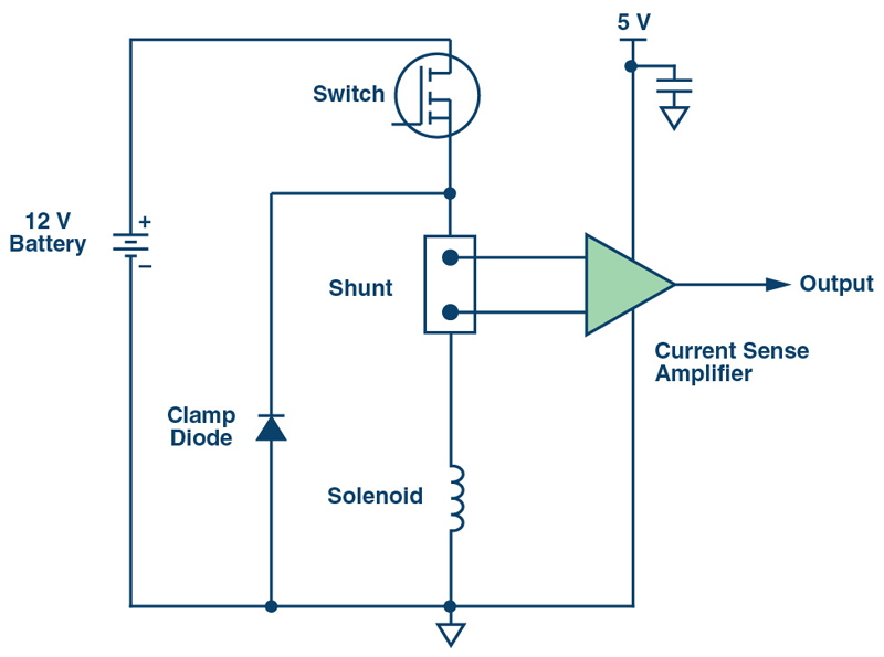
Click image to enlarge
Figure 1. High-Side Current Sensing in Solenoid Control Application
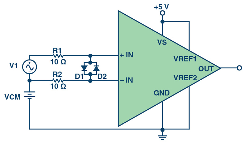
Overvoltage protection circuit
Figure 2 shows the basic connection for overvoltage protection of a current sense amplifier. When the differential input voltage exceeds the maximum rated value for a given amplifier, the amplifier may begin to pull current into the internal protection diodes. The additional series resistors, R1 and R2, prevent large current flow to the internal protection diodes if a large differential voltage signal is present between the input pins.
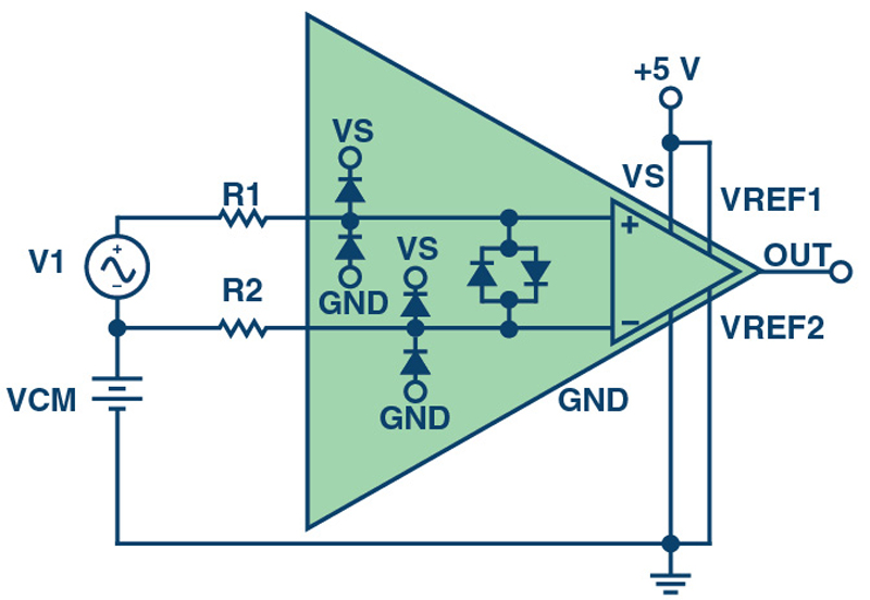
Click image to enlarge
Figure 2. Basic Overvoltage Protection Circuit
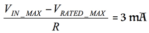
Both the maximum rated voltage and the maximum input current tolerated by a protection circuit vary from device to device. As a general rule of thumb, limit the current passing through the internal differential protection diodes to 3 mA unless there is a specification indicating a larger value is acceptable. Given this value, calculate the values of R1 and R2 using Equation 1.
where:
VIN_MAX is the expected maximum differential voltage.
VRATED_MAX is the maximum rated voltage (0.7 V).
R is the total series resistance (R1 + R2).
For example, if the expected maximum transient input voltage is 10 V, the equation is
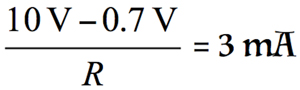
If R = 3.1 kΩ, then based on Equation 1, R1 and R2 = 1.55 kΩ.
These values for R1 and R2 are significant, relative to the input impedance of certain amplifiers, and can contribute a large error to the overall system performance. One way to reduce the value of R1 and R2 is to add external protection diodes with higher current capabilities on the input pins, as shown in Figure 3.
Click image to enlarge
Figure 3. Overvoltage Protection Circuit with External Input Differential Protection Diodes
For example, when using the Digi-Key B0520LW-7-F Schottky diode, which can handle up to 500 mA of forward current, the value of R is reduced to 20 Ω
Trade-offs in system performance
Adding series resistors to the input of the amplifier can degrade certain performance parameters. In some amplifiers, R1 and R2 appear in series with internal precision resistors. In other amplifiers, offset currents work with the resistors to create offset voltages. The parameters most likely to be affected are gain error, common-mode rejection ratio (CMRR), and offset voltage.
To examine the potential impact of the series resistance, measurements were taken on two current sense amplifiers configured with protection resistors at the input pins. The test setup used for evaluating gain error, CMRR, and offset voltage is shown in Figure 4. This setup uses the Agilent E3631A power supply for providing the 5 V single-supply to the device, the Yokogawa GS200 precision dc source for the differential input voltage signal, the HAMEG HMP4030 for setting the CMV, and the Agilent 3458A precision multimeter for measuring the output voltage of the current sense amplifiers.
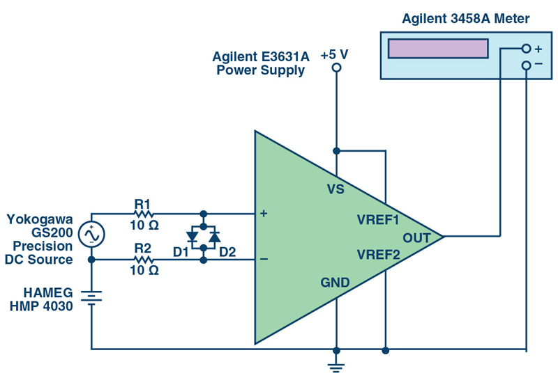
Click image to enlarge
Figure 4. Test Setup for Evaluating the Gain Error, CMRR, and Offset Voltage
Both the AD8210 and the AD8418 were evaluated to measure the impact of the additional series resistors on the gain error, CMRR, and offset voltage parameters of the devicesGain error
When series resistors are placed in series with the input of an amplifier, they form a resistor divider with the differential input impedance of the amplifier. The resistor divider introduces an attenuation that appears at the circuit level as additional gain error. The additional gain error will be larger for amplifiers with lower differential input impedances.
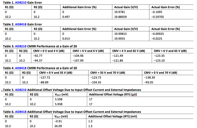
Table 1 shows the calculated, additional gain error and the actual gain error of the AD8210. The AD8418 was tested with and without the protection circuit as well. Table 2 shows the calculated additional gain error and the actual gain error of the amplifier.
Click image to enlarge
In the measured results, the AD8418 gain error shifts by .013% while the AD8210 shifts by 0.497 %. The input impedances of the AD8418 and AD8210 are 150 kΩ and 2 kΩ respectively so it follows that the error introduced in the AD8418 would be less than the AD8210.
Common-mode rejection ratio
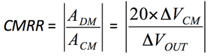
Because current sense amplifiers are usually exposed to environments with high CMV, CMRR is one of the most important specifications. CMRR assesses the ability of a device to reject high CMVs and attain optimal accuracy and performance. It refers to a measure of change in output voltage when equal voltage is applied at the two input terminals of the amplifier. CMRR is defined as a ratio of the differential gain to the common-mode gain and is usually specified in decibels.
Use Equation 3 and Equation 4 to find the CMRR values for both amplifiers.

where:
ADM is the differential gain of the AD8210 and the AD8418 (ADM = 20).
ACM is the common-mode gain, ΔVOUT/ΔVCM.
When series resistors are in series with the input of an amplifier, the mismatch of the series resistors is added to any mismatch of the internal resistors, which will impact the CMRR.
The CMRR measurement results for the AD8210 and the AD8418 current sense amplifiers are shown in Table 3 and Table 4, respectively. (above)
The results indicate that the effect of the additional external series resistors is a reduction in the AD8418 CMRR and has a smaller effect on the AD8210 CMRR. The AD8418 moved to 89 dB while the AD8210 remained almost unchanged at 94 dB. The common mode impedance of both amplifier is relatively high for fixed gain devices, with the AD8418 and AD8210 at 750kΩ and 5MΩ respectively.
Offset voltage
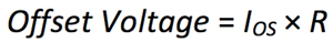
When bias currents pass through the external resistors, they produce an error voltage in series with the intrinsic offset voltage of the device. To compute this additional offset voltage error, multiply the input offset current (IOS), the difference between the two input bias currents, by the external impedance present on the input pins, as shown in Equation 5.
where:
IOS is the input offset current.
R is the additional external impedance.
The increase in offset voltage based on measurements from the AD8210 and the AD8418 current sense amplifiers are shown in Table 5 and Table 6, respectively.
The results show that the increase in offset voltage in the AD8418 is larger than the increase in offset voltage in the AD8210. This is caused by the input offset current of the AD8418, which is around 100 μA. Any additional impedances in series the input pins, together with the input offset current, create an additional offset voltage error.
Protection is performance
Implementing additional series resistors on the input pins is a simple way to protect a current sense amplifier against overvoltage conditions. The impact on performance measures such as gain error, CMRR, and offset voltage is measurable and directly related to the magnitude of the external resistors and the type of current sense amplifier used. If designed properly, the circuit improves the application’s differential input voltage ratings with a modest increase in component count and a minimal impact on precision.