Designing with Silicon Carbide in Bidirectional On-Board Chargers
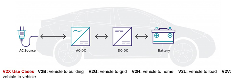
Figure 1: A bidirectional OBC enables new vehicle-to-everything use cases
Electric vehicle (EV) on-board chargers (OBCs) can take several forms based on power level and functions. Charging powers vary from less than 2 kW in applications such as electric scooters to 22 kW in high-end EVs. Traditionally, charging power is unidirectional, but bi-directional charging is gaining traction.
Why bidirectional OBCs?
As EVs operating purely on electric power continue to increase market share, the installed battery capacity per vehicle is also increasing. Consumers are demanding faster charging times for larger-capacity batteries. This demand is spurring an increase in battery operating voltage from 400 V to 800 V, beginning with high-performance vehicles.
An EV equipped with sufficient battery capacity is potentially capable of acting as an energy-storage system, enabling a variety of vehicle-to-everything charging use cases: vehicle-to-home power generation, vehicle-to-grid opportunities, or vehicle-to-vehicle charging. As a result, the OBC is migrating from a unidirectional to a bidirectional topology.
Bidirectional OBC system blocks
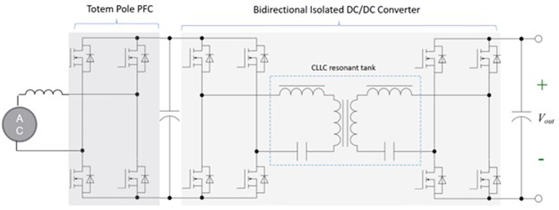
An OBC design for an EV requires high power density and maximized efficiency to make the most of available EV space and minimize weight. Abidirectional OBC consists of a bidirectional AC/DC converter, typically a power-factor–correction (PFC) or active front end (AFE) circuit followed by an isolated bidirectional DC/DC converter. Let’s examine these separately.
PFC/AFE block
A conventional PFC boost converter is the most widely used topology for single-phase use, but it does not support bidirectional operation and is inefficient. The totem-pole PFC improves efficiency by eliminating the bridge rectifier stage, reducing the number of semiconductor devices in the conduction path from three to two.
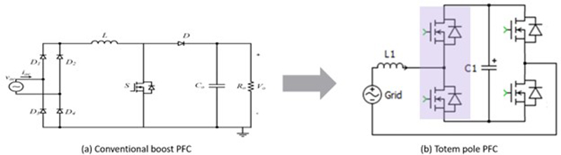
Click image to enlarge
Figure 2: Changing from a boost topology (a) to a totem-pole PFC (b) improves efficiency and allows for bidirectional operation.
The totem-pole PFC contains two sections (legs) that operate at different frequencies. The high-speed leg boosts the voltage and shapes the current; this leg must switch at a high frequency. The low-speed leg primarily rectifies the input voltage and can switch at the line frequency of 50/60 Hz.
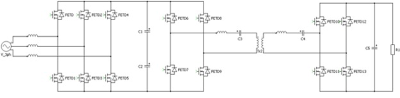
In some regions in Europe, three phase power is available for residential utility, typically three phase 6 switch PFC/AFE topology can be used.
Click image to enlarge
Figure 3. Bi-directional three phase 6 switch PFC topology
There are other types of three phase PFC such as T-type PFC, which is a 3-level converter. The benefits of the 3-level converter are lower switching loss and smaller inductor size. These benefits come with increased complexity of the system, more component counts, higher cost and overall size of the converter. The basic 2 level three phase PFC converter is the most commonly used topology for three phase bi-directional OBC.
DC/DC converter block
The DC/DC converter in aunidirectional OBC is typically an LLC resonant converter, but this is a unidirectional topology: in reverse operation mode, the voltage gain of the converter is limited, reducing its performance. A bidirectional CLLC resonant converter is preferred for the DC/DC stage, as it combines high efficiency with a wide output voltage range in both charging and discharging modes.
Click image to enlarge
Figure 4. Bi-directional CLLC DCDC converter
In an EV OBC application, the CLLC employs soft switching for higher efficiency: zero-voltage switching (ZVS) on the primary side and ZVS combined with zero-current switching on the secondary side.
A common bi-directional DCDC converter topology is dual active bridge (DAB). DAB’ s operation is simple, regulating output by phase shifting. It has limited range of ZVS, and higher switching loss than CLLC since DAB turn-off current is higher than CLLC. In general, DAB has lower efficiency than CLLC but, the design of resonant circuit in CLLC is more complicated.
The many advantages of Silicon Carbide
SiC is preferred for high-power systems due to its unique combination of high critical electric field, high electron drift velocity, high temperature, and high thermal conductivity. This leads to a low on-state resistance (RDS(on)) and low switching loss making it ideal for high-current high voltage applications.
There are two other options for the active devices in a high-power design: silicon (Si) MOSFETS and Si IGBTs. A Si MOSFET is impractical for high-power applications in the totem-pole PFC. The reverse recovery of the Si MOSFET body diode leads to high power losses in continuous-conduction mode (CCM), so its use is restricted to discontinuous-mode operation and low-power applications. A SiC MOSFET allows the totem-pole PFC to operate in CCM for high efficiency, low EMI, and increased power density. For the voltage rating, Si MOSFET can have good Rdson performance up to 650 V. For 1200 V class, Si MOSFET’s Rdson will be too high for such high-power applications.
A SiC MOSFET has advantages over an IGBT. The IGBT does not contain a body diode; an ultra-fast diode may be used instead, but the IGBT’s maximum switching frequency is limited due to its high switching loss. The low switching frequency increases the weight and size of the magnetics and passive components compared with a SiC solution.
Medium-power bidirectional OBC architecture (<6.6 kW)
A medium-power OBC typically operates from a single-phase 120 V or 240 V input with a 400 V DC bus. The topology is single phase totem pole PFC followed by a CLLC DCDC converter.
Click image to enlarge
Figure 5: High-efficiency OBC architecture using SiC and a totem-pole PFC
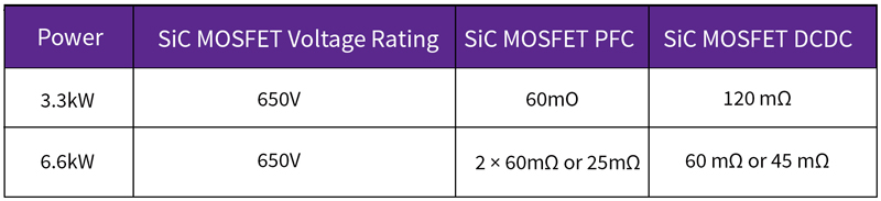
For 6.6 kW, two 60 mΩ MOSFET (e.g. E3M0060065K) in parallel or one 25 mΩ can be used for each position in PFC and one 60 mΩ (E3M0060065K) or 45 mΩ (e.g. E3M0045065K) device for each position in DCDC.
Click image to enlarge
Table 1. MOSFET choices for high-efficiency bi-directional OBC architecture (3.3–6.6 kW)
Higher-power bidirectional OBC designs (11 kW/22 kW)
At higher power levels, the battery voltage can be either 400 V or 800 V, but the market is trending toward 800 V.
The 11 kW design can use 75 mΩ 1200 V MOSFET (e.g. E3M0075120K) for PFC and the primary side of the CLLC converter. On the secondary side, an 800V battery application uses the same 75 mΩ MOSFETs as the primary. 40 mΩ 1200 V MOSFET can be used for high performance applications. For a 400 V battery application, four 650 V 25 mΩ MOSFETs can be selected for the secondary side.
The 22kW design mirrors that of the 11 kW OBC, but the higher power output requires lower Rdson devices. A 32 mΩ 1200 V MOSFET will be used for PFC and primary side of DCDC. The secondary side can either use the same primary-side devices for 800 V bus applications or substitute 650 V 15 mΩ for 400 V applications.
Click image to enlarge
Table 2: MOSFET choices for 11kW and 22kW Bi-directional OBC
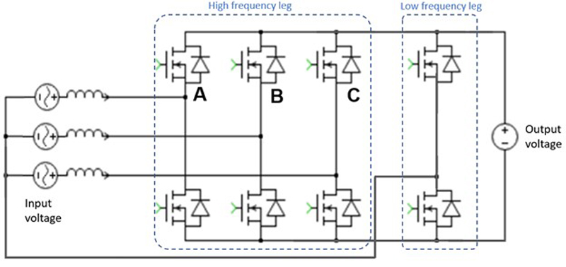
22 kW Silicon Carbide-based design with single-phase input and three phase input
In many European homes, three-phase power is readily available, but typical U.S. homes, Asian and South American homes have only a 240 V single-phase, where the design calls for a high-power 22 kW OBC, which can be compatible with both single phase and three phases to reduce OBC SKU. A fourth leg is added to conventional three phase (leg) PFC such that the designer can use an interleaving technique for single phase input. The high-frequency leg of each PFC supplies 6.6 kW via 32 mΩ 1200 V SiC MOSFETs. The low-frequency leg uses two Si IGBTs to reduce cost. When three phase is available, this circuit automatically re-configures itself to three phase operation, leaving the fourth leg floating.
Summary
Bidirectional function is the new trend in EV OBC designs. Wolfspeed SiC MOSFETs address many power-design challenges by providing devices with low on-resistance, very low output capacitance, and low source inductance for a perfect blend of low switching losses and low conduction losses. Compared with Si-based solutions, Wolfspeed SiC power-device technology enables increased system power density, higher switching frequencies, reduced component count and size of components such as inductors, capacitors, filters, and transformers, and potential system cost reduction. Wolfspeed has created multiple bi-directional OBC reference designs, including 6.6kW and 22kW. Please visit reference design page in Wolfspeed.com for more information.