Pushing the Power Density Envelope in DC/DC Conversion
High-level system performance with next-gen hybrid switched-capacitor high-density (HSC-HD) converters with truly differential input (TDI) gate driver ICs
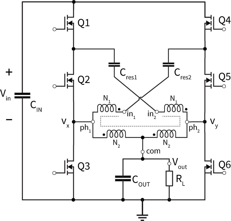
Figure 1a
One of the biggest challenges in enabling Artificial Intelligence (AI) computing is the increase of processing power in a fixed converter footprint. As a consequence, such intense power demands are shifting rack power levels above the 30-kW range. The “Open Compute Project” (OCP) attempts to address these challenges by defining new standards at the power architecture level, moving from traditional 12 V power distribution to 48 V at the rack level. Since galvanic isolation is unnecessary in this voltage domain, new DC/DC power converter topologies and devices are being researched and enabled.
In today’s 48 V power architecture, a two-stage approach is commonly adopted to satisfy both high step-down ratio requirements and transient performances. In this architecture, typically, the first stage acts as DCX (fixed ratio) intermediate bus converter (IBC), and the second stage is a voltage regulation module (VRM) implemented with a multiphase buck converter for accurate voltage regulation.
In a traditional accelerator card for data center and computing applications based on artificial intelligence (AI), the available footprint area for the IBC and multiphase buck is limited. Therefore, high switching frequency operation is needed both at the first and second stages. However, the high switching frequency on the VRM stage would lead to high losses (i.e., switching, driving, core, and conduction losses). Hence a high-ratio DCX converter is necessary to maintain full system efficiency and power density.
As a high-ratio DCX converter, Infineon has recently introduced a hybrid switched-capacitor (HSC) converter, illustrated in figure 1. This converter combines the benefits of a non-isolated converter and the high step-down conversion capability of a multi-tapped autotransformer (MTA). HSC converter offers high performance by transferring energy through capacitors and a magnetic, reducing the overall stress on magnetic and power MOSFETs. However, the DC/DC converter topology level innovation alone cannot keep up with the power density required in AI applications.

Click image to enlarge Figure 1b
Figures 1a & 1b: HSC topology (a) and HSC-HD hardware implementation (b)
A Key Enabler for High Power Density
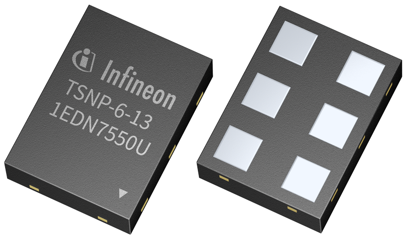
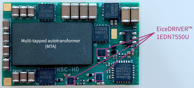
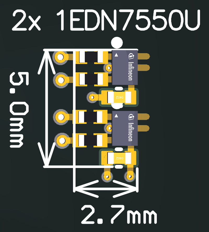
The HSC-HD converter in figure 1 is a 500 W dual-phase multi-level resonant converter capable of 98% peak efficiency with 2.2 kW/in² power density. According to the topology shown, four high-side single-channel gate driver ICs in a small form factor are required to enable the power density above. To support this need, Infineon has recently introduced the EiceDRIVER 1EDN7550U single-channel non-isolated gate driver IC with truly differential input (TDI) in ultra-small package, as shown in figure 2 (a).
Click image to enlarge
Figures 2a & 2b: EiceDRIVER 1EDN7550U in a TSNP 1.1x1.5 mm2 package (a) and placement on HSC-HD top side (b)
The TDI feature makes both high-side and low-side driving possible while enabling the smallest industry footprint for a single-channel driver when compared to other gate-driving solutions.
The EiceDRIVER 1EDN7550U gate driver IC provides several benefits in the HSC-HD converter and other multi-level topologies in general. These benefits include:
• Capability to directly drive high-side switches thanks to TDI
• Ultra-small driving-stage area in the TSNP package size 1.1 x 1.5 mm². The overall layout area is less than 14 mm² per switch, including the common-mode resistors and the supply bypass capacitor
• Versatile placement of the driver for better optimization of area, driving loop, or both
• 50 percent RthJB reduction when compared to all other packages available on the market
• Significative cost saving compared to galvanic isolated gate driver ICs.
Using TDI to Achieve High-Side Driving
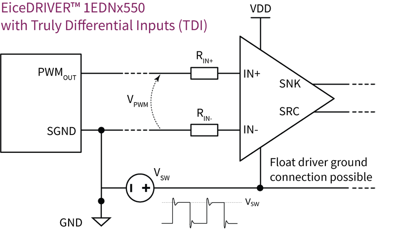
The key feature of the EiceDRIVER 1EDN7550U is the TDI stage. It differs substantially from generic single-channel non-isolated gate driver ICs, as the TDI stage allows driving high-side switches without using bulky, expensive, and over-specified functional isolated drivers.
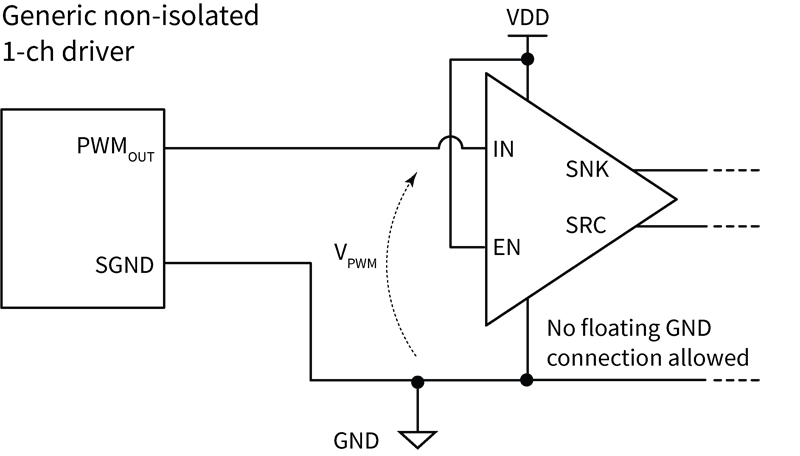
The working principle of the TDI input stage is similar to a differential amplifier. As shown in figure 3(b), the differential input stage enables communication with the driver without the need for signal shifting. Therefore, it is capable of rejecting common-mode voltage with respect to GND up to the configured common-mode robustness (CMR). Consequently, this driver can be reliably used to drive high-side switches as the switching node voltage VSW will be rejected as common-mode “noise” thanks to the TDI stage.
Click image to enlarge
Figures 3a & 3b: Input PWM voltage detection in a standard single-channel non-isolated driver (a) and in EiceDRIVER 1EDN7550U (b) with TDI
The driving configuration for the power MOSFETs Q1, Q2, and Q3 in the HSC topology is shown in figure 4. The driving stage of the power MOSFETs Q4, Q5, and Q6 is symmetric.

Click image to enlarge
Figure 4: Application example of EiceDRIVER 1EDN7550U in the HSC topology
As shown, the digital outputs of the controller can be directly connected to the EiceDRIVER 1EDN7550U through small series resistors.
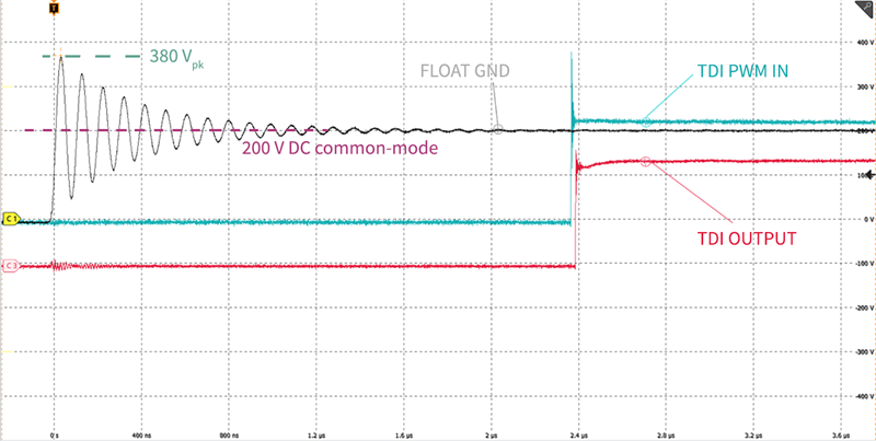
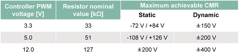
The CMR defines the maximum common-mode voltage that the TDI stage can reject. This parameter can be configured by placing the two small resistors, RIN+ and RIN-, upstream of the input pins. By selecting the proper value, tolerance, and form factor, CMR up to static ±200 V (phase node nominal voltage) and dynamic ±400 V (phase node ringing) can be achieved.
Figure 5 shows the CMR capabilities of the EiceDRIVER 1EDN7550U. Clean switching of the driver can be achieved (TDI PWM input in cyan, TDI output in red) when applying a 400 V ringing or a 200 V DC offset to the floating ground of the driver (black color) by means of a LC resonator. The maximum achievable CMRs are reported in table 1. Infineon’s EiceDRIVER 1EDNx550 device datasheet includes an explanation of how to configure the driver for the required CMR.
Click image to enlarge
Figures 5a and b: Common-mode rejection test on the TDI input stage of EiceDRIVER 1EDN7550U
In the HSC topology (figure 1), the maximum common-mode voltage experienced by each 1EDN7550U floating ground equals the source voltage of the transistors Q1, Q4, Q2, and Q5, as the driving PWM signals are referenced to GND together with the microcontroller IC. For Q1 and Q4, the DC common-mode voltage equals the maximum input voltage VIN = 60 V, while for Q2 and Q5, it equals Vx and Vy voltages during Q3 and Q6 turn-off, that is, VIN,max /4 = 15 V.
Once the maximum common-mode voltage and the controller PWM voltage are known, the required static CMR parameter of the TDI stage can be configured in order to drive the high-side switches.
Pushing the Driving Stage to Dot-Size
An area comparison can be performed between the dual-channel isolated EiceDRIVER 2EDF7275K and the single-channel EiceDRIVER 1EDN7550U to illustrate the space benefits of TSNP packages at the system level.
Both the EiceDRIVER 2EDF7275K and the EiceDRIVER 1EDN7550U can operate the high-side switches in the HSC topology. In particular, switches Q1, Q2, Q4, and Q5 can be driven either using two dual-channel isolated drivers, such as the EiceDRIVER 2EDF7275K, or four single-channel TDI non-isolated drivers as the EiceDRIVER 1EDN7550U.
The overall driving areas required for two switches are:
• 35 mm² for 1x EiceDRIVER 2EDF7275K including all passives
• 13.5 mm² for 2x EiceDRIVER 1EDN7550U, including all passives and input resistors.
Figure 6 shows that a 50 percent driving stage area reduction is possible with EiceDRIVER 1EDN7550U, enabling better layout, transformer arrangement, and thermal dissipation in high power density DC/DC converters.

Click image to enlarge
Figures 6a & 6b: Driving area comparison between the dual-channel isolated solution (a) and EiceDRIVER 1EDN7550U (b)
Click image to enlarge
Table 1: Maximum common-mode voltage rejected from the EiceDRIVER 1EDN7550U vs. input resistor nominal value
Furthermore, since the 1EDN7550U is a single-channel driver, it allows higher layout versatility as each driver can be placed separately. This results in one more degree of freedom for the designer during placement, and the hardware can then be optimized for area occupation, driving loop, or both.
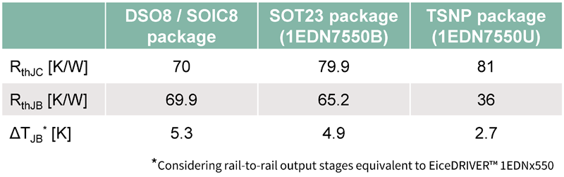
Low thermal resistance TSNP packages
In many power designs, the inner copper layers of the PCB are used to extract heat from the power MOSFETs and mitigate the temperature rise in the power stage. This is especially true for the ground planes when source down MOSFETs are used as synchronous rectifier (SR) MOSFETs. This widely used temperature-spreading technique benefits the whole system with regard to reliability and overall efficiency. However, it dramatically increases the temperature of copper planes, which is the PCB reference temperature for both power MOSFETs and gate drivers. Therefore, to keep a low Tj for the gate driver ICs, a low RthJB is highly desirable to achieve the lowest possible ΔTJB.
Click image to enlarge
Table 2: Typical thermal performances for different industry packages
Thermal performance is firstly improved through the EiceDRIVER 1EDN7550U low-ohmic output stage, whose typical RDS(on),SRC of 0.85 Ω and RDS(on),SNK 0.35 Ω enables reduction of power dissipation inside the driver. Furthermore, the thermal capabilities of the TSNP package allow an additional 50 percent reduction of RthJB when compared to other packages.
By combining the low-ohmic output stage of the EiceDRIVER 1EDN7550x with the high thermal performance of the TSNP package, the ΔTJB can be minimized. This reduces driving losses and improves overall system reliability.