Qualifying SiC Devices to Industrial and Auto Standards
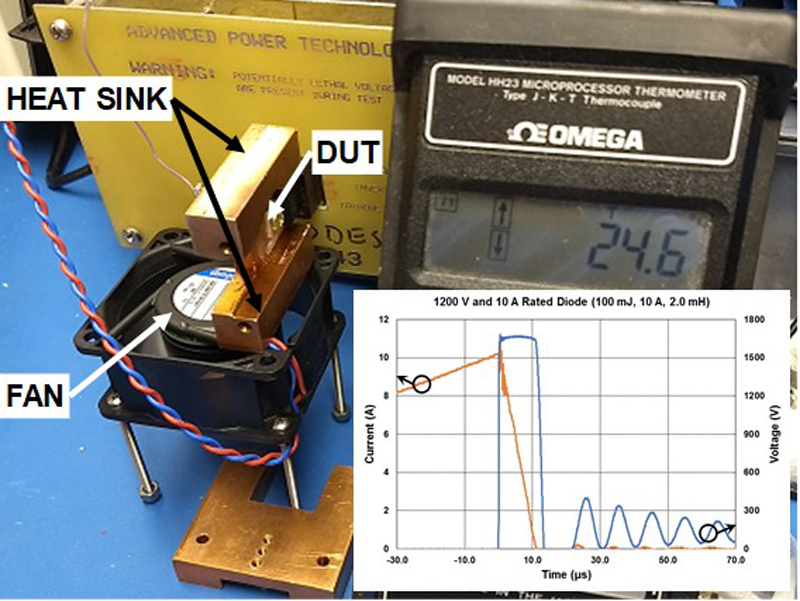
Figure 1: RUIS test setup and waveforms for the current and the voltage during a UIS pulse.
A recent trend in the semiconductor market is the widespread adoption of silicon carbide (SiC) devices, including both Schottky barrier diodes (SBD) and power MOSFETs, for industrial and automotive applications. At the same time, the long-term reliability of these devices is a hot topic that should be addressed since there is limited field data to analyze. Some SiC providers have begun qualifying SiC devices to stringent industrial and automotive (AEC-Q101) standards, and others have even gone beyond the qualification standards requirements to also provide data for harsh ruggedness tests. This qualification and testing strategy, combined with the use of specific design rules for achieving high Avalanche ruggedness, are critical in order for SiC devices to sustain their fast adoption rates in mission- and safety-critical applications.
Rapid Market Growth
The growth in market share for SiC devices is expected to accelerate in the coming years, with the main driver being the electrification in the transportation sector. SiC dies will be an essential building block in modules for applications such as on-board chargers and powertrain traction systems. Thanks to the high critical electric field for avalanche breakdown, high-voltage SiC devices have a much smaller footprint than their silicon counterparts and can operate at higher switching frequencies. SiC’s thermal properties are also very attractive, with an excellent heat dissipation and the ability to operate at elevated temperatures. In practice, the maximum operating temperature is typically 175°C and rarely exceeds 200°C, the main limitation being the assembly process (soldering metal, package material). SiC devices are inherently more efficient than silicon ones, and the number of individual dies in a module can be drastically reduced by switching to SiC dies.
As SiC devices move from niche to mainstream markets, the main challenges associated with the ramp-up to high volume manufacturing are being overcome. To ease this transition, fabrication plants are setting up SiC lines sharing tools with pre-existing silicon lines. This arrangement allows the cost to be lowered for the SiC dies as the overhead would be shared with Si. Recent constraints on wafer availability are becoming less of an issue with significant capacity increases by wafer vendors. Continuous improvements in 4H-SiC substrate and epitaxy growth lead to high-quality 6-inch wafers with a low density of crystal defects. The high quality of the wafers translates into high yield for SiC devices at electrical parameters tests.
It is important to remember, though, that that there is limited reliability data from the field for these devices since they have only been commercially available for a few years. Also, the qualification of SiC devices has been significantly more arduous than that of silicon devices, with its own set of challenges. The electric field in reverse bias condition is close to one order of magnitude higher in SiC devices. Without proper design rules, this high electric field could easily damage the gate oxide. The density of traps near the gate oxide interface is also much higher for SiC. As a result, instabilities might arise during burn-in tests as traps get electrically charged. A persistent focus on long-term reliability improvement has yielded reassuring results, with recent reports of devices qualified to stringent industrial and automotive (AEC-Q101) standards.
In addition to this, SiC providers have begun taking the next step by providing data for harsh ruggedness tests.
Harsh Ruggedness Testing
An example of this harsh ruggedness testing was performed by Microchip, through its Microsemi subsidiary, on its SiC SBDs and MOSFETs for 700, 1200, and 1700 V voltage nodes. The tests identified that a high level of unclamped inductive switching (UIS) ruggedness is critical to guarantee the long-term reliability of a part. They showed that, during a UIS test, there is a high transient current that flows through a reverse-biased device and drives it into avalanche breakdown. The combined effect of high current and voltage results in significant heat generation and a sharp increase in temperature. Locally, the maximum temperature could reach up to 500°C for a rugged power MOSFET, well above a typical temperature rating.
The UIS ruggedness has a strong dependence on the quality of the epitaxy and the manufacturing process, both front end and back end of the line. Even small crystal defects in the epitaxy or process-related defects could constitute weak spots where a device would fail prematurely during a UIS test. This is why a thorough analysis of the ruggedness of a product family should include both single-pulse and repetitive UIS (RUIS) testing.
The single-pulse test is implemented as a screening test to identify parts with low UIS ruggedness. To guarantee a UIS rating in a product’s datasheet, all the parts should be tested before being shipped to customers. However, a part is likely to undergo multiple UIS events during its lifetime in the field. To characterize the gradual wear-out, repetitive tests are required. For in-depth characterization, a part should be submitted to a high number of pulses, with 100,000 hits being a common practice.
During a UIS pulse, the current in the device under test decreases continuously while the voltage remains essentially constant but for slight variations due to thermal effects (Figure 1). The energy of a UIS pulse is defined by both the maximum current at the beginning of the pulse and the inductance of the load. In the test procedure, the energy was adjusted by varying the value of the inductance. The maximum current was kept constant; it is equal to the forward current rating for SBDs and to two-thirds of the drain current rating for MOSFETs.
RUIS tests have specific constraints, mainly to prevent the build-up of the temperature from one pulse to the next. It is important to ensure that the temperature of the device is near the ambient temperature before applying a new pulse. In the test setup shown in Figure 1, the temperature of the part is monitored with a thermo-couple sensor and the pulse repetition rate is adjusted to get a constant reading. To help the part to cool down, it is mounted on a heat sink and placed under a fan.
Device Design for High Avalanche Ruggedness
In addition to adopting proper testing procedures, best-in-class UIS ruggedness also requires using the following set of design rules:
- The high-voltage termination is designed with a high enough intrinsic breakdown voltage to ensure the active area goes into avalanche first. Under this condition, the energy is dissipated over the whole active area and not in the narrow termination, which would lead to a premature failure.
- The shielding of the electric field in the JFET region of the MOSFET is critical to protect the gate oxide. The design and the implant scheme of the P-doped wells delimiting the JFET region should be carefully optimized to provide an adequate shielding without strongly impacting the on-state resistance.
- A passivation material with high thermal conductivity provides a path for the heat to diffuse through the top side of the die.
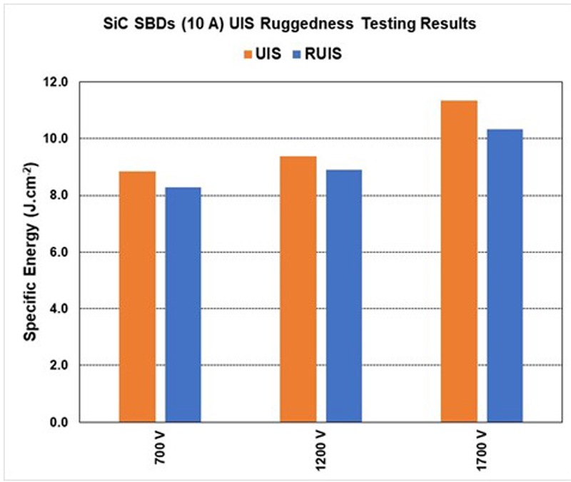
Both Schottky diodes and power MOSFETs that were designed using these rules perform well in harsh ruggedness tests. SBDs were tested up to failure for single-pulse and repetitive UIS, and several DC parameters were monitored. Results of this testing show that the forward voltage and reverse leakage current of the devices remain very stable while the reverse breakdown voltage increases slightly, which can be attributed to free carriers trapping near the SiC top surface. The energies of the pulses right before failure are shown in Figure 2. The UIS ruggedness increases with the voltage rating of the part. This trend can be explained considering that most of the heat generation happens in the epitaxy region. As the epitaxy thickness increases with the voltage rating, the heat generation per unit of volume decreases, which in turn reduces the temperature in the device. The UIS ruggedness is also systematically lower for repetitive tests, but to a small extent. The difference compared to single-pulse UIS is smaller than 10 percent. The multiple UIS pulses do not have a strong cumulative effect, and it is expected that the SBDs will remain rugged over their entire lifetimes in the field.
Click image to enlarge
Figure 2: Specific energy per active area before failure for 700, 1200, and 1700 V SiC SBDs.
MOSFET characterization for harsh ruggedness should focus on the gate oxide long-term reliability, which does not require stressing the parts up to failure. Instead, a repetitive test consisting of 100,000 pulses of relatively low energy was used. An example is a Microsemi 1200 V / 40 mΩ MOSFET that was designed using rules for Avalanche ruggedness, and was tested with 100 mJ pulses; while it’s single pulse UIS rating is 2.0 J. Most DC parameters were not affected; however, this test stressed the gate oxide, and a moderate increase in gate leakage was observed. To determine if the long-term reliability was compromised, the parts were submitted to a time-dependent dielectric breakdown. The times to failure with 50 µA DC current on the gate are reported in Figure 3 for a combination of parts including the Microsemi SiC devices that were developed using the company’s Avalanche ruggedness rules, and those from three other leading suppliers.

Click image to enlarge
Figure 3: TDDB times to failure for 1200 V MOSFETs from four providers.
Keeping SiC Adoption on Course
The adoption of SiC devices in the industrial and automotive markets has come with stringent long-term reliability requirements. The optimum strategy for addressing these requirements is to qualify products with the automotive AEC-Q101 standard and perform characterizations for extreme ruggedness tests that have not yet been standardized, as well. Also important is the application of design rules for high Avalanche ruggedness. Together, these steps will help ensure that SiC devices not only continue on their fast adoption path, but also deliver the long-term reliability that these applications demand
Microsemi Corporation


