Redefining Power Conversion with Gallium Nitride ICs
Gallium nitride (GaN) power devices have been in production for more than a decade.
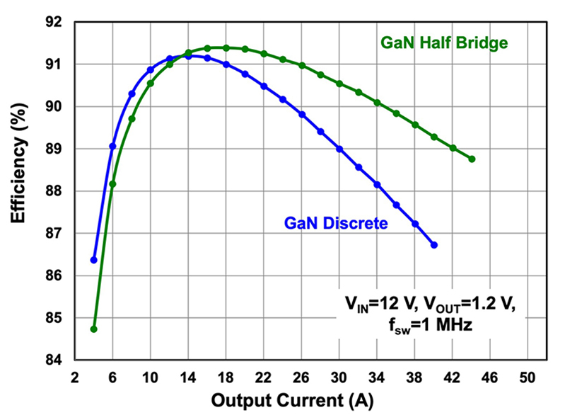
Figure 1: Performance comparison of GaN discrete (blue line) and GaN monolithich half bridge (green line) in a 12 V input, 12 V output buck converter operating at 1 MHz.
Beyond just performance and cost improvements, the most significant opportunity for GaN technology to impact the power conversion market comes from the intrinsic ability to integrate multiple devices on the same substrate. This capability will allow monolithic power systems to be designed on a single chip in a more straightforward, higher efficiency, and more cost-effective way.
GaN-based ICs have gone through various phases of integration, from pure discrete devices to monolithic half-bridge devices, to power FETs that included their own monolithically integrated driver, and, more recently, to fully monolithic power stages containing power FETs, drivers, level shifting circuits, logic, and protection.
Phase One: Monolithic Half Bridges
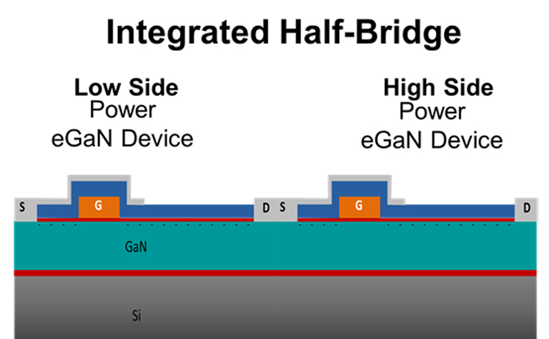
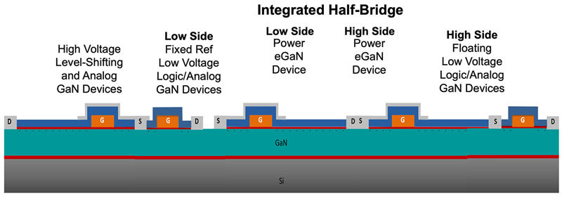
Approximately six years ago, EPC started its first phase of integration with the monolithic half bridge. The compelling reason for this first step was that the half bridge is the most common building block used in power conversion. The first IC devices put both the high-side and low-side transistors onto one substrate as shown in Figure 2. The advantages of integration included the reduction in size and cost, and, by virtue of the close coupling of the two transistors, the parasitic common source inductances were also reduced. Also, the advantage of increased switching speed enables even faster and more efficient switching power conversion systems while the reduced power loop inductance lowered the voltage overshoot at the switch node and resultant EMI.

Click image to enlarge
Figure 2 a & 2b: Cross section diagram of an integrated half bridge and (b) die images of a selection of 30 V – 100 V symmetrical and asymmetrical half bridges
Figure 1 compares the performance of discrete devices versus a monolithic half bridge device in a buck converter with an input voltage of 12 volts and an output voltage of 1.2 volts operating at 1 MHz. The blue line represents the result from two GaN discrete transistors being driven by a silicon driver in a very efficient layout on a PCB board. The green line represents the performance of the monolithic half-bridge device.
The efficiency for the monolithic solution is much higher for multiple reasons. The first reason is that the power loop inductance has been reduced from about 400 pH to about the 200 pH range and, when operating at a megahertz, that makes a significant impact. The second reason is that in an asymmetric buck converter, the high-side device or control device tends to run hotter than the low-side device. When those two devices are together on the same chip, they balance each other thermally and can achieve a lower peak temperature, and an overall better efficiency.
Phase Two: eGaN FET Plus Driver
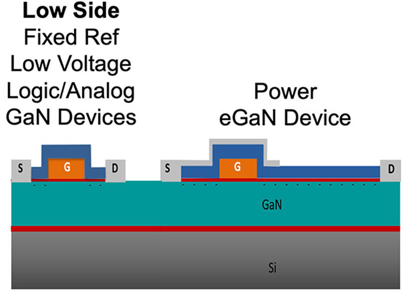
In gallium nitride, the distance between the gate and the drain largely determines the voltage that the device can withstand. By shrinking that distance, a much smaller device can be made, which also enables the location of very simple, low-voltage logic and analog devices on the same chip with the high power, high voltage devices as shown in figure 3.
Click image to enlarge
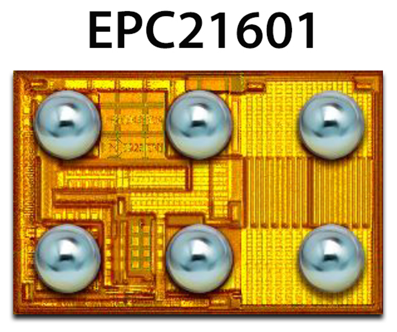
Figures 3a and 3b: Cross section diagram of an integrated eGaN FET plus driver (b) die image of the EPC21601, a time-of-flight eGaN FET plus driver IC
Figure 3b shows an example of the EPC21601, an eGaN FET plus driver integration in a time-of-flight (ToF) IC. On the left-hand side of the chip, the circuit with input logic, as well as drivers, for the FET are visible. On the right-hand side, the output FET is visible. This device will take a logic signal and send out a very high current and a very, very short pulse to fire a laser in a time-of-flight lidar application. This is an excellent example of how integrating the driver plus the GaN field effect transistor on one chip generates an extremely powerful and very fast IC that can be driven off a regular logic gate.
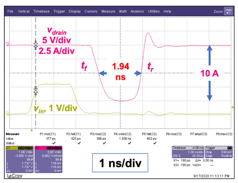
Figure 4 shows the result of this integration. The pink line in the graph shows the drain current through the device. It shows a 10-ampere pulse that is about 1.94 nanoseconds wide and has a rise time of 380 picoseconds and a fall time of 525 picoseconds. When the 2.1 V logic input signal – the green line – is enabling the device, there is about a one nanosecond delay between the input signal and the output. That is blazing fast! This device can comfortably operate at a 100-megahertz pulse frequency.
Click image to enlarge
Figure 4: Single pulse waveform 2.1 V logic level input. The yellow trace is input (1 V/div) and the pink line is drain current (5 V/div or 2.5 A/div).
Phase Three: ePower Stage
In early 2019, the driver function and the monolithic half bridge were merged onto a single GaN-on-silicon substrate along with a level shifter, synchronous boost circuit, protection, and input logic as shown in figure 5. A photo of this device, the EPC2152, is shown in figure 6. This complete power stage, the ePower Stage, can be driven at multi-megahertz frequencies and controlled by a simple low-side CMOS IC and, with just a few added passive components, can become a complete DC-DC regulator. This solution is 35% smaller and has half the number of components compared to a discrete implementation. The integrated power stage requires a lot less design time, because this is simply logic in and power out.
Click image to enlarge
Figure 5: Cross section diagram of an eGaN integrated power stage

Click image to enlarge
Figure 6: Die image of the EPC2152, ePower Stage
Figure 7 shows the efficiency and power loss of this monolithic power stage) at 500 kHz in a bidirectional 48 VIN – 12 VOUT, 300 W, 1/16TH brick converter. The blue line shows the efficiency of the EPC9151 converter, and the green line represents the power loss.
There are three factors that attribute to higher performance with the monolithic power stage. First, the power loop inductance is significantly reduced by making a monolithic half bridge. Secondly, the gate loop inductance in eliminated by putting the drivers on the same chip located extremely close to the FETs. Lastly, by putting all these components together, a thermal tub is created that balances the temperature of all the devices, so there is a net, on average, lower temperature. Video of this demonstration can be found on the EPC website.

Click image to enlarge
Figure 7: Measured efficiency and loss for the EPC9151 1/16th brick converter: (a) VIN = 48 V, VOUT = 12 V (buck); and (b) VIN= 12 V, VOUT = 48 V (boost)
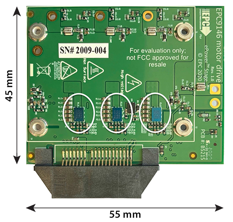
In addition, the integrated power stage has been tested in a three-phase motor drive application, pictured in figure 8. The advantage in this application is the ability to go to a much higher switching frequency for the motor drive, which reduces size (this solution is only 45 mm by 55 mm), reduces weight, reduces audible noise, and provides much higher precision in the positioning of the motor. The positioning of motors is critical for many robotic implementations.
Click image to enlarge
Figure 8: photo of 500 W, three-phase motor drive circuit using the EPC2152, ePower Stage (circled)
The Future of GaN
Figure 9 shows a summary of the ongoing eGaN technology journey. EPC is in generation ”five plus” of its discrete platform, illustrated in the top bar of figure 9. Regarding integrated circuits, what started with monolithic half bridges has subsequently expanded to add more functions and features as illustrated in the bottom bar of figure 9.
The monolithic power stage IC discussed in the previous section performs all the same basic functions as a multi-chip DrMOS module based on silicon MOSFETs, but at higher voltages, higher switching speed, in a smaller footprint, and at lower cost. These first-generation power stages only include capacitors, resistors and lateral n-channel FETs. Soon additional sensing of current and temperature can be included along with circuit blocks such as references, comparators, and op amps to construct an integrated controller plus output stage on a single chip. Multi-level topologies can also be integrated, thus enabling higher input voltages with lower voltage power devices.

Click image to enlarge
Figure 9: Roadmap for GaN technology discrete and integration development
In a few years, the merging of discrete technology to integrated circuits will occur. As discrete devices achieve increasingly higher power densities, it will no longer be possible to extract the current in and out of the bumps and bars on the devices. Therefore, integration into small, multi-chip, multi-function integrated circuits will be necessary. It is likely that within the next three to four years the slow obsolescence of discrete transistors in power conversion will occur and integrated solutions will be the component that designers select when building a power system.
Summary
EPC’s eGaN technology is developing rapidly with frequent releases of new generations of discrete devices that become the platform for new generations of more efficient, smaller, and lower cost integrated circuits. GaN integrated circuits make products smaller, faster, more efficient, and easier to design. The ascent of GaN is redefining power conversion, and integrated circuits have the biggest impact from this great new technology!