Researchers Developed a Universal Dual Metal Precursor Method to Grow Non-Layered 2D Materials
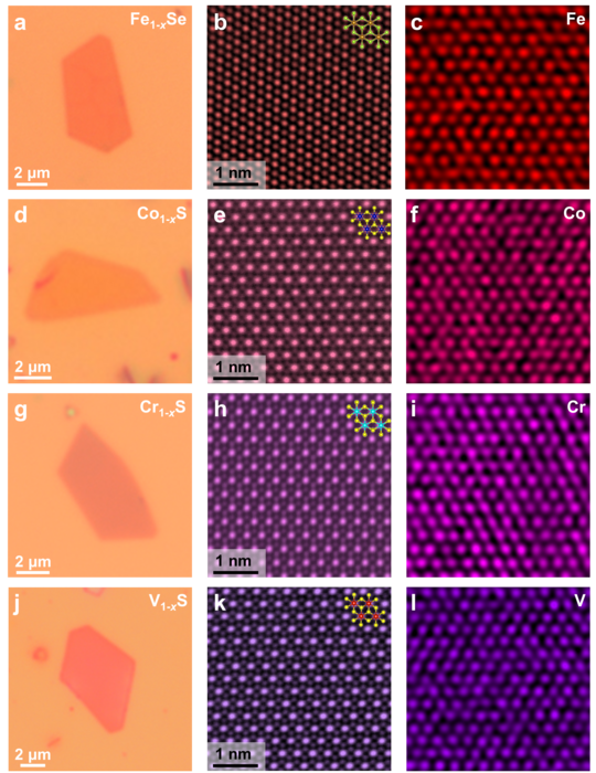
Two-dimensional transition metal chalcogenides (2D TMCs) have drawn great interest due to their abundant material choices and possible use in many areas like electronics and optoelectronics. As a complement to the widely-studied layered TMCs (e.g., MoS2), non-layered TMCs are unique due to their unsaturated dangling bonds on the surface and strong intralayer and interlayer bonding. So far, limited by established preparation methods, the investigations of these non-layered TMC materials mainly remained on bulks or polycrystalline films, hindering the exploration of their physical characteristic and properties at 2D thickness limit. In a recent paper published in Science Bulletin, a group led by Profs. Bilu Liu and Hui-Ming Cheng from Tsinghua-Berkeley Shenzhen Institute (TBSI) of Tsinghua University and Profs. Junhao Lin and Yue Zhao of Southern University of Science and Technology have developed a novel dual-metal precursors method, which realizes the controllable growth of various non-layered 2D TMCs, including Fe1-xS, Fe1-xSe, Co1-xS, Cr1-xS, and V1-xS.
In this dual metal growth method, the mixture of low-melting-point metal chloride and the corresponding high-melting-point metal powder was used as the dual-metal precursors. During the gas-phase reaction process, the evaporation rate was well controlled to provide a constant metal source feed and facilitate the growth of non-layered 2D TMCs with thin thickness. Taking hexagonal Fe1–xS as an example, the thickness is down to 3 nm with a lateral size up to >100 μm.
Thanks to the ultrathin nature and flat surface of the obtained flakes, the structure and transport behaviors of Fe1-xS at the 2D thickness limit were measured at the first time. Advanced microscopy inspections revreal that intrinsic ordered cation vacancies exist in the non-layered TMC family. In stark contrast, anion vacancies (S, Se, and Te) are well-known dominant point defects in common layered TMCs like MoS2. Low-temperature transport measurements and theoretical calculations reveal that 2D Fe1–xS is a semiconductor with a narrow bandgap of 20–60 meV. Compared to other narrow bandgap 2D materials like 1T'-MoTe2 and black phosphorus, 2D Fe1–xS shows better air stability and thermal stability. This work essentially solves the problem of growing ultrathin non-layered materials, and thus provides material basis for both fundamental study and applications of these emerging family of non-layered 2D materials.
This work was supported by the National Science Fund for Distinguished Young Scholars (52125309), the National Natural Science Foundation of China (51991343, 51920105002, 51991340, 52188101, and 11974156), Guangdong Innovative and Entrepreneurial Research Team Program (2017ZT07C341 and 2019ZT08C044), the Bureau of Industry and Information Technology of Shenzhen for the ‘‘2017 Graphene Manufacturing Innovation Center Project” (201901171523), Shenzhen Basic Research Project (JCYJ20200109144616617 and JCYJ20190809180605522), and Shenzhen Science and Technology Program (KQTD2 0190929173815000 and 20200925161102001). The authors acknowledge the assistance of SUSTech Core Research Facilities, especially technical support from Pico-Centre. This work was also assisted by the professional FIB-TEM consulting services provided by Hong Kong Ultravision holdings Co., Limited.
EurekAlert!, the online, global news service operated by AAAS, the science society.