
As artificial intelligence (AI) and high-performance computing continue to proliferate, the physical infrastructure of data centers is struggling to keep up.
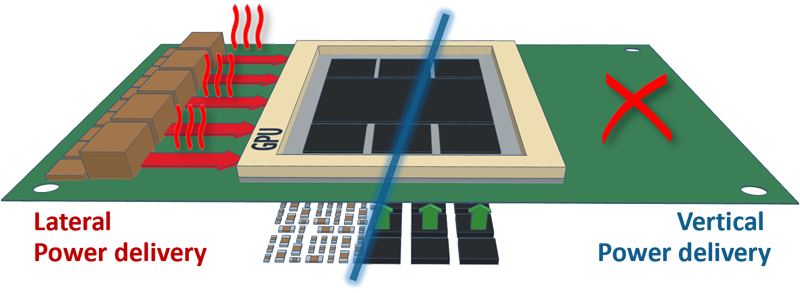
Figure 1: LPD moves current through one layer from the board’s edge to its center
Each generation of accelerators, whether GPUs, AI engines, or XPUs, consumes more power than the last, pushing the limits of what engineers have designed server architectures to support. In fact, a single inference request to a generative model today consumes ten times more energy than a conventional web search. Multiply that by billions of queries per day, and the energy implications become impossible to ignore.
At the same time, this surge in compute demand is colliding with an inability to efficiently deliver high-current, low-voltage power to processors. While chipmakers continue to shrink geometries and increase transistor density, power delivery architectures have remained largely static. The result is a growing disconnect between what chips are capable of and what infrastructure can support. Nowhere is this more evident than at the final stage of power delivery, where current can exceed thousands of amps into millimeters of silicon.
To unlock the true power of artificial intelligence, the industry needs to fundamentally reconsider power delivery. This article explores the limits of conventional lateral power delivery (LPD) and why a reimagined approach, true vertical power delivery (VPD), could be the answer.
The Limits of Lateral Power Delivery
In a traditional system, DC/DC converters mounted on the printed circuit board (PCB) convert 12V rails to the sub-1V levels required by processors. These converters often sit several centimeters away from the chip, with power routed laterally across the board. For decades, LPD served as the default architecture for converting and distributing power within data center servers. While this paradigm has worked thus far, it’s now starting to collapse under the weight of modern compute demands.
The problem is rooted in physics. As supply voltages shrink and current requirements swell, the I2R losses from even short trace lengths become intolerable. Lateral routing introduces parasitic resistance and inductance that collectively erode power efficiency and throttle performance. Power lost in the distribution system (PCB) exceeds 10% of the system power budget, defeating the best efforts of the high-efficiency voltage regulators and compounding the thermal challenges.
Worse still, traditional converters are inherently bulky. Their slow switching speeds necessitate large magnetic components and massive banks of decoupling capacitors that often consume the most valuable real estate beneath the processor. Engineers must space these components around thermal constraints like heat spreaders, which further increase the distance to the load and degrade transient response. While a large bank of capacitors can support a fast load step to limit the immediate droop in voltage, their recovery is orders of magnitude slower, driven by the slowness and distance of the voltage regulators from these capacitors.
The result is cascading inefficiency. Poor voltage regulation leads to higher voltage margins, which means more energy is burned just to ensure operation. A 50-millivolt reduction in the voltage margin for an xPU running at 0.75V can result in over 10% savings in dynamic power loss. A slow recovery transient response force xPUs to throttle performance or enter recovery cycles. In aggregate, LPD is no longer a viable pathway for high-throughput, power-hungry AI workloads.
The Shift to 48V and Multi-Stage Conversion
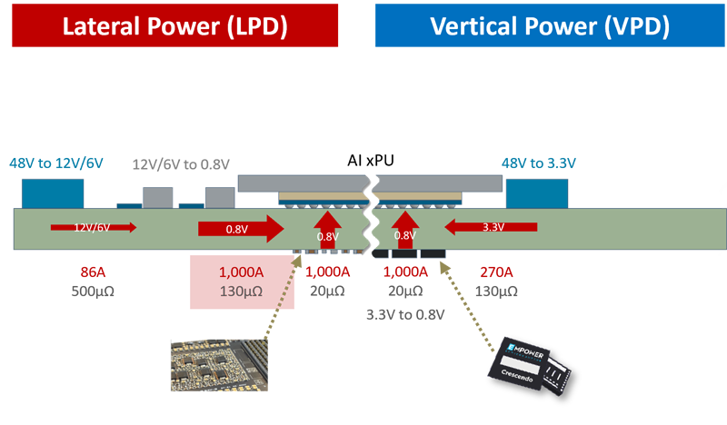
To address growing energy demands and transmission losses, data centers have undergone a profound transition from 12V to 48V busbars within a rack to distribute power to the individual rack units. The principle is straightforward: higher voltage requires less current to deliver the same power, which in turn reduces resistive losses and shrinks the size of the power delivery infrastructure. Cables, connectors, and busbars become smaller and cooler, which simplifies system-level design and lowers the total cost of ownership.
However, this shift introduces new architectural complexity. While the power delivery now occurs at 48V, the processing cores still require sub-1V inputs. While converting 48V directly to the core voltage in a single step is not impossible, given the extreme duty cycle (Vout / Vin) ratio, such a conversion leads to a large, bulky system.
As a result, systems now demand a two-stage conversion. First, 48V is converted to an intermediate voltage (commonly 12V), and then the 12V is stepped down to the final point-of-load voltage.
In order to optimize the power delivery at the “last-inch”, it is practical to continue to stick to the 2-stage approach, as a lower input voltage 2nd stage can provide a much higher density, thinner, and higher bandwidth solution.
This second stage, where conversion to 0.7V or lower occurs, is where most of the performance, space, and thermal challenges now concentrate.
The Density Problem in AI Architectures
An additional challenge is that the escalating compute demands of modern AI workloads in turn escalate the physical constraints surrounding power delivery.
On large xPU packages, a significant fraction of pins is allocated to high-speed communication and I/O, leaving a relatively small area available for power delivery, even as total current requirements surge into thousands of amps. The result is a sharp increase in current density: more current must be delivered through fewer pins and smaller board real estate, dramatically raising the stakes for efficiency, thermal management, and voltage regulation.
This challenge is amplified in many next-generation AI system architectures that deploy multiple xPUs in tightly packed grids or tiled arrangements, where high-speed interconnects between tiles are a bottleneck for system performance. To maintain signal integrity and reduce latency, these interconnects must remain short and unobstructed. But this imposes a hard constraint on power delivery, where regulators must deliver high current without encroaching on lateral PCB space, whether on the top side near heat spreaders or on the bottom side near interconnect routing.
In these environments, traditional power modules that consume valuable footprint or height are no longer viable. Instead, the power delivery system must adapt to the physical structure of the compute plane, conforming to tight spatial constraints while maintaining bandwidth, response time, and efficiency.
True Vertical Power Delivery as the Answer
To address the growing inefficiencies of lateral power delivery, system architects are increasingly exploring VPD as the next architectural shift. Rather than routing power across the PCB from distant converters, VPD delivers current through the board stack directly into the silicon, reducing resistive losses, minimizing parasitics, and dramatically improving transient response.
The value behind VPD is simply that shorter distances mean fewer losses. But realizing that in practice is far more complex. A truly vertical architecture must compress the power delivery solution into the same footprint, and ideally the same vertical space, as the processor itself. That means eliminating the bulky magnetics, capacitors, and lateral routing paths that characterize traditional power stages.
Click image to enlarge
Figure 2: Vertical power delivery sends current through the board stack directly into the silicon
Yet many so-called “vertical” solutions available today fall short of that standard. Some simply invert existing lateral converters and mount them on the underside of the board. Others shift the converter closer to the load but retain large banks of decoupling capacitors that consume valuable space and limit placement flexibility. These designs may offer incremental improvements, but they fail to solve the underlying problem of delivering large currents with nanosecond response directly to sub-1V rails, without degrading density.
True VPD requires an architectural rethink. It must be compact enough to live beneath the processor, fast enough to eliminate capacitor banks, and scalable enough to support the growing demands of AI-class workloads. Without all three, the system still suffers from the same constraints, just rearranged into a slightly different form.
The Key to Achieving True Vertical Power Delivery
Any viable VPD solution must solve three interrelated challenges: bandwidth, efficiency, and mechanical integration.
Eliminating the Capacitor Bank, a Bandwidth & Density Challenge
A defining feature of traditional designs is their reliance on large banks of decoupling capacitors to manage high-frequency transients. These capacitors consume large amounts of area beneath the processor and are incompatible with true vertical power. They also degrade the solution density of a power delivery solution. To remove them, the voltage regulator must exhibit significantly higher bandwidth.
Most legacy voltage regulators operate in the 500–800 kHz range, which is far too slow to react to sub-microsecond current steps. For true VPD, the control loop must cross over into the multi-megahertz regime, allowing the regulator to directly absorb fast transients without relying on external capacitive energy storage. Eliminating the capacitor bank is also a major step to matching the current density required by the xPU. Most modern xPU packages have a significant amount of embedded capacitors in them, representing the package PDN impedance. If a voltage regulator can close the gap with bandwidth that exceeds the package PDN’s crossover frequency, that eliminates more than 95% of PCB capacitors, allowing the active power delivery solution to be realized as true vertical power.
Maintaining Efficiency at Scale
Beyond requiring high-speed regulation and density, true vertical power delivery necessitates efficient voltage regulators. Specifically, any second-stage voltage regulator operating near the processor must achieve benchmark efficiency, typically above 90%, to avoid thermal buildup and offsetting the system-level gains made through 48V intermediate busbar distribution. This becomes especially important as current requirements exceed 1,000 amps, as even marginal efficiency losses result in significant heat and wasted power.
Mechanical and Thermal Constraints
Relocating power delivery to the PCB backside introduces tight packaging constraints. Solutions must conform to standardized thickness envelopes dictated by form factors like OCP OAM and PCIe. That means the total height, including power stages, magnetics, and any thermal interface, must remain within 2–4 mm. At the same time, these thin-profile regulators must still dissipate significant heat, necessitating dual-side cooling options or integrated low-impedance thermal paths to maintain reliability.
Crescendo Platform with FinFast Technology
The new Crescendo platform delivers true VPD that solves all previously stated challenges. Rather than retrofitting conventional architectures, this new platform redefines the power stage itself by compressing all essential elements into a dense, low-profile form factor designed to operate directly beneath the processor.
Based on Empower’s FinFastTM technology, the Crescendo platform features high-frequency IVRs with integrated magnetics in a 6 mm x 7 mm package as thin as 1.25 mm. Importantly, this integration eliminates the need for large external inductors and decoupling capacitors to create the physical and electrical conditions necessary for vertical delivery. By mounting on the PCB backside, the solution delivers current vertically through vias to the processor die, shortening the path, tightening voltage regulation, and dramatically improving transient response.
Click image to enlarge
Figure 3: The Crescendo Platform enables true vertical power delivery to a processor
Performance gains are substantial. Transient response improves by up to 20x compared to conventional converters, with peak current delivery scalable beyond 3,000 amps through module paralleling. The architecture also supports up to 5x greater power density and enables system-level power loss savings of up to 20%. Meanwhile, the removal of under-processor capacitor banks frees board space and reduces thermal congestion so that system designers can increase compute density or simplify board layouts.
Most importantly, this new platform is implemented with commonly available foundry processes, components and packaging. For system architects tasked with delivering kW level power to processors with high density, the platform offers a practical, immediate, and performance-proven solution to the most pressing power bottlenecks in AI and HPC infrastructure.
Click image to enlarge
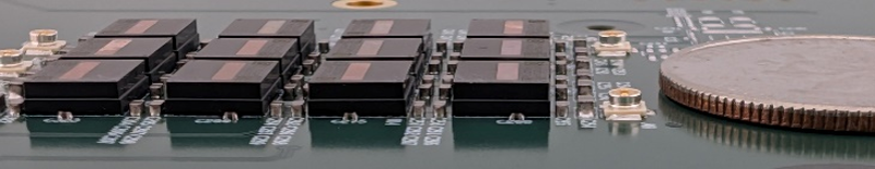
Figure 4: The Crescendo Platform implemented on the bottom side of PCB (under xPU)
Conclusion
Whereas computing performance has always been constrained by transistor counts or core frequency, today it’s constrained by power delivery. As AI accelerators grow more capable, they also demand unprecedented amounts of power at increasingly lower voltages, within increasingly confined mechanical envelopes. The industry has responded with higher-voltage rack distribution, intermediate bus architectures, and new packaging strategies, but these only go so far. The final stage, where energy meets silicon, remains the most important and least forgiving.
VPD is a promising solution to that challenge. But as the term gains popularity, clarity becomes more important. Simply re-purposing existing slow power modules to the backside of the board does not constitute VPD. Instead, VPD must truly shrink the power delivery loop to enable fast response, dense packaging, and the removal of bulky passives that have long constrained placement and performance. The Crescendo platform is one of the few technologies to meet that bar.


