Reducing Capacitance Requirements in Your Power Supplies
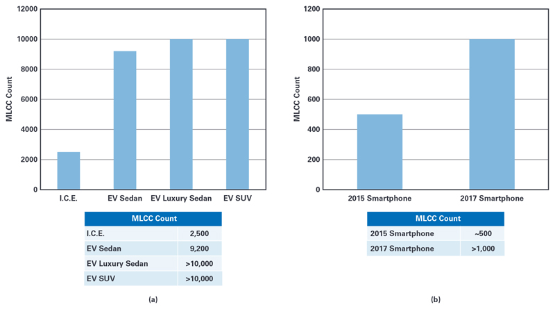
Figure 1. Increases in worldwide MLCC use in electric automobiles (a) and cell phones (b), without commensurate increases in production, have led to shortages.
The worldwide supply of multilayer ceramic capacitors (MLCCs) is not keeping up with demand. This is due in no small part to increased electronic complexity of cell phones, increased sales of electric cars, and a worldwide expansion of electronic content across industries. Some smartphones have doubled MLCC usage over a few years; an electric vehicle can quadruple usage over a typical modern internal combustion engine (Figure 1). The supply shortage of MLCCs, appearing near the end of 2016, has made it especially difficult to obtain large-capacity products (several tens of µF or more) necessary for the operation of prolific power supplies used in the latest electronics. Manufacturers looking to reduce their MLCC requirements inevitably look to the capacitor requirements of power supplies—in particular, switching regulators. This places power supply designers on the front lines of mitigating the cap shortage.
Power Circuits Use Capacitors, A Lot of Capacitors
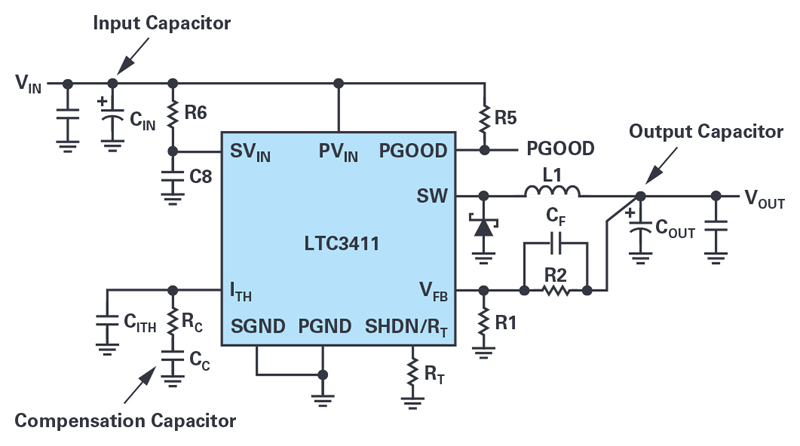
A typical dc-to-dc buck converter uses the following capacitors (see Figure 2):
· Output capacitor: Smooths out both output voltage ripple and supply load current during load transients. Generally, a large capacitor measuring several tens of μF to 100 μF is used.
· Input capacitor: In addition to stabilizing the input voltage, it plays theroleofinstantaneouslysupplyingtheinputcurrent.Ingeneral,several μF to several tens of μF areused.
· Bypass capacitor: Absorbs noise generated by switching operation and noise from other circuits. 0.01 μF to 0.1 μF are generally used.
· Compensation capacitor: It secures the phase margin in the feedback loop and prevents oscillation. Several hundreds of pF or several tens of nF are often used. Some switching regulator ICs incorporate the compensation capacitor.
Click image to enlarge
Figure 2. Capacitors used in a typical buck regulator
The best way to reduce capacitance is to focus on minimizing the output capacitors. A strategy for reducing output capacitance is explored next, followed by solutions to reducing bypass capacitor requirements and, to some extent, input capacitors.
Increase Switching Frequency to ReduceOutput Capacitance
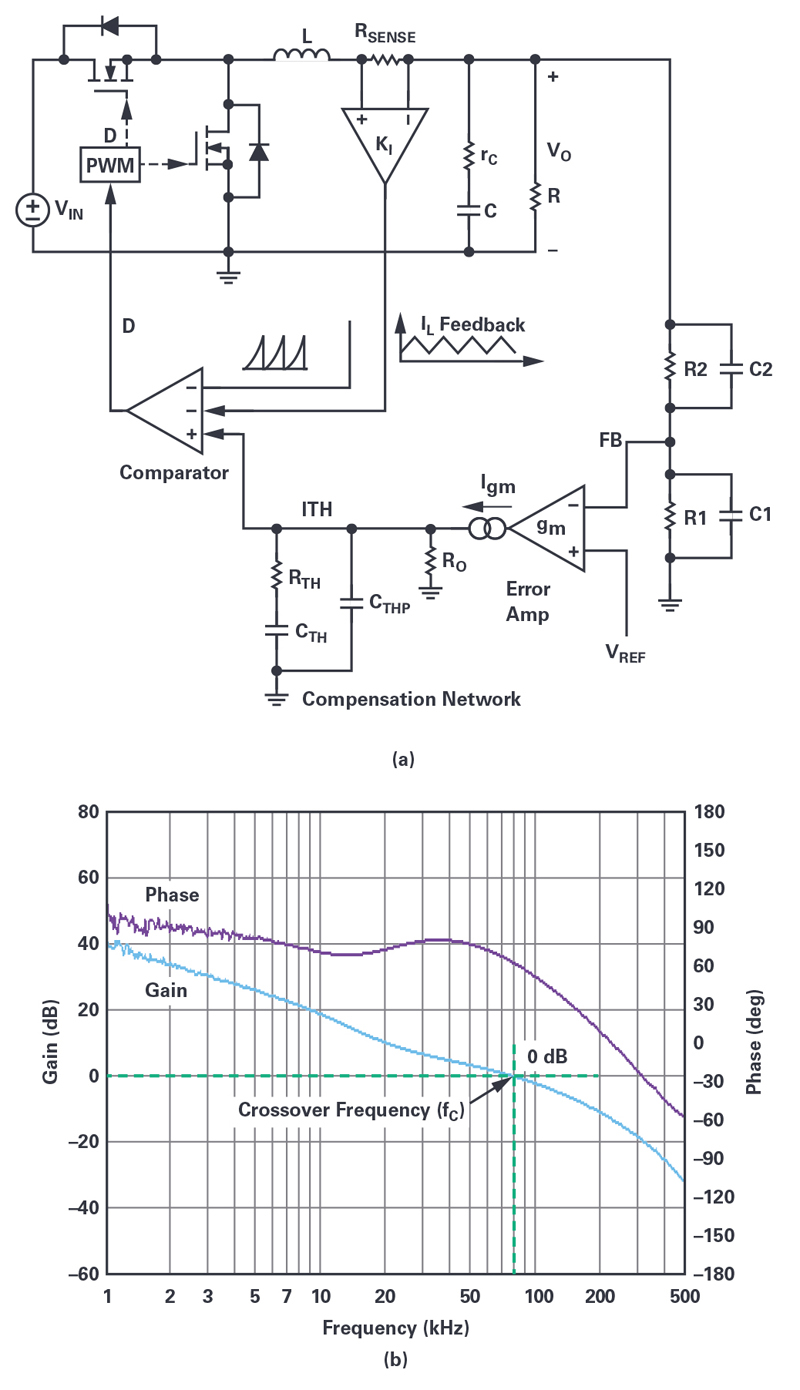
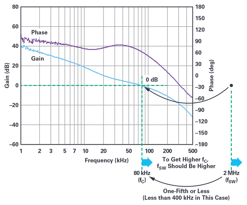
Figure 3a shows a typical current-mode buck converter block diagram, with the shaded area denoting the feedback loop and the compensation circuit.
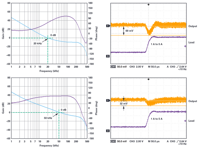
The characteristic of the feedback loop is shown in Figure 3b. The frequency at which the loop gain is 0dB (gain=1) is called the crossover frequency (fC). The higher the crossover frequency, the better the load step response of the regulator. For example, Figure 4 shows the load step response for a regulator supporting a rapid load current increase from 1 A to 5 A. The results are shown for crossover frequencies of 20kHz and 50kHz, resulting in 60mV and 32 mV dropouts, respectively.
Click image to enlarge
Figure 3. Block diagram of a typical buck regulator (a) and typical feedback characteristic (b)
Click image to enlarge
Figure 4. Comparing the load step responses of a buck regulator at two crossover frequencies
On the surface, increasing the crossover frequency looks like an easy choice: load step response is improved by minimizing the output voltage drop, so the output capacitor can be reduced. Raising the crossover frequency, though, brings up two issues. First, it is necessary to secure a sufficient phase margin of the feedback loop to prevent oscillation. Generally, a phase margin of 45° or more (preferably 60° or more) is required at the crossover frequency.
The other issue is the relationship between switching frequency (fSW) and fc. If they are similar in magnitude, negative feedback can respond to the output voltage ripple, threatening stable operation. As a guideline, set the crossover frequency to one-fifth (or less) of the switching frequency, as shown in Figure 5.
Click image to enlarge
Figure 5. If the switching frequency and control loop crossover frequency are too close, the negative feedback may respond to output voltage ripple. It is best to keep the crossover frequency below one-fifth of the switching frequency
To increase the crossover frequency, you must also raise the switching frequency, which in turn results in higher switching losses via the top and bottom FETs, reducing conversion efficiency and generating additional heat. Any savings in capacitance is offset by the complexity of additional heat mitigation components: fins, fans, or additional board space.
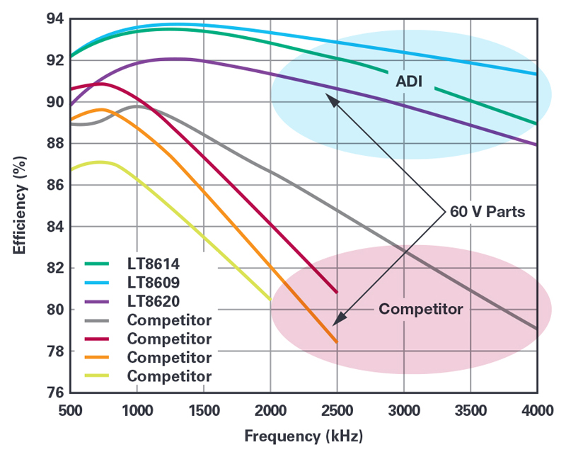
Is it possible to maintain high efficiency at high frequency operation? The answer is yes. A number of Power by Linear regulator ICs from Analog Devices do just that by incorporating a unique FET control that keeps efficiency high even at higher switching frequencies (Figure 6).
Click image to enlarge
Figure 6. Power by Linear regulators vs. competition. In a typical regulator, when the switching frequency goes up, efficiency goes down. ADI Power by Linear regulators can maintain high efficiency at very high operating frequencies, enabling the use of smaller value output capacitors
For example, the LT8640S 6 A output buck regulator maintains greater than 90% efficiency over its full load range (0.5 A to 6 A) while operating at a frequency of 2 MHz (12 V input and 5 V output).
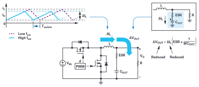
This regulator also lowers the capacitance requirements by reducing inductor current ripple (ΔIL), which in turn reduces the output ripple voltage (ΔVOUT) as shown in Figure 7. Likewise, a much smaller inductor can be used.
Click image to enlarge
Figure 7. Increase switching frequencies to reduce capacitor and inductor size
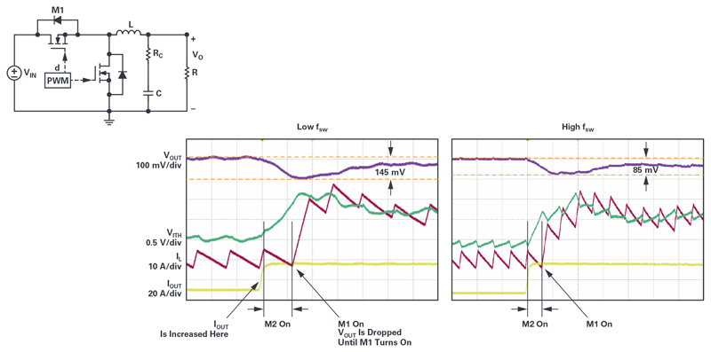
With a higher switching frequency, the crossover frequency can be increased, improving load step response and load regulation, as shown in Figure 8.
Click image to enlarge
Figure 8. Increased switching frequency results in improved load step response
Silent Switcher Regulators Significantly Reduce Bypass Capacitance
How about reducing bypass capacitance? The main role of the bypass capacitor is to absorb the noise generated by switching operation itself. If switching noise is reduced in other ways, the number of bypass capacitors can be reduced. A particularly easy way to achieve this is through the use of a Silent Switcher regulator.
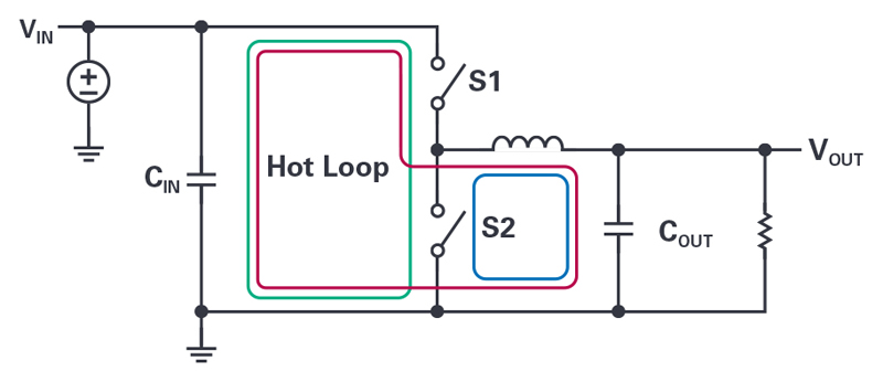
How does a Silent Switcher regulator reduce switching noise? A switching regulator has two current loops: When the top FET is on and the bottom FET is off (red loop) and when the top FET is off and the bottom FET is on (blue loop) as shown in Figure 9. The hot loop carries a fully switched ac current — that is, switched from zero to IPEAK and back to zero. It has the highest ac and EMI energy, as it produces the strongest changing magnetic field.
Click image to enlarge
Figure 9. The hot loop in a switching regulator produces the bulk of the radiated noise because of the alternating magnetic field it generates
Slew-rate control can be used to suppress switching noise by slowing the rate of change of the gate signals (lowering di/dt). While effective in suppressing the noise, this increases switching losses, producing additional heat, especially at high switching frequencies as previously described. Slew-rate control is effective under certain conditions and Analog Devices also offers solutions with this feature.
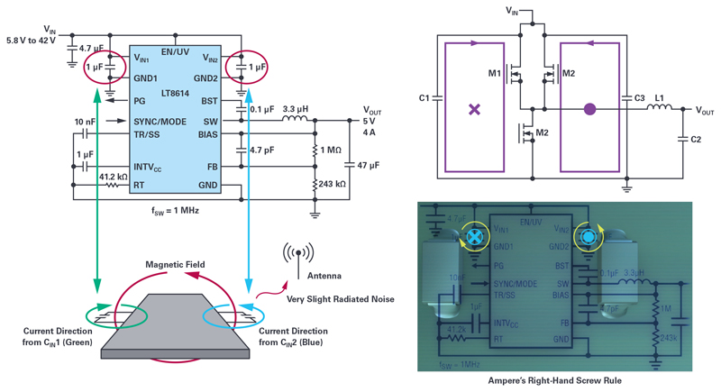
Silent Switcher regulators suppress electromagnetic noise generated from the hot loop without slew-rate control. Rather, it splits the VIN pin in two, allowing the hot loop to be split into two symmetrical hot loops. The resulting magnetic field is confined to the area near the IC, and significantly reduced elsewhere, thus minimizing radiated switching noise (Figure 10).
Click image to enlarge
Figure 10. Patented Silent Switcher technology
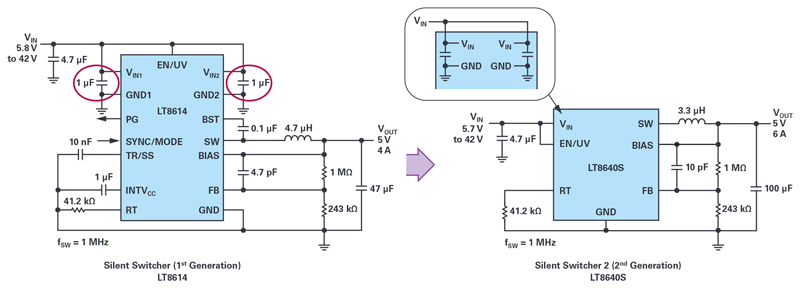
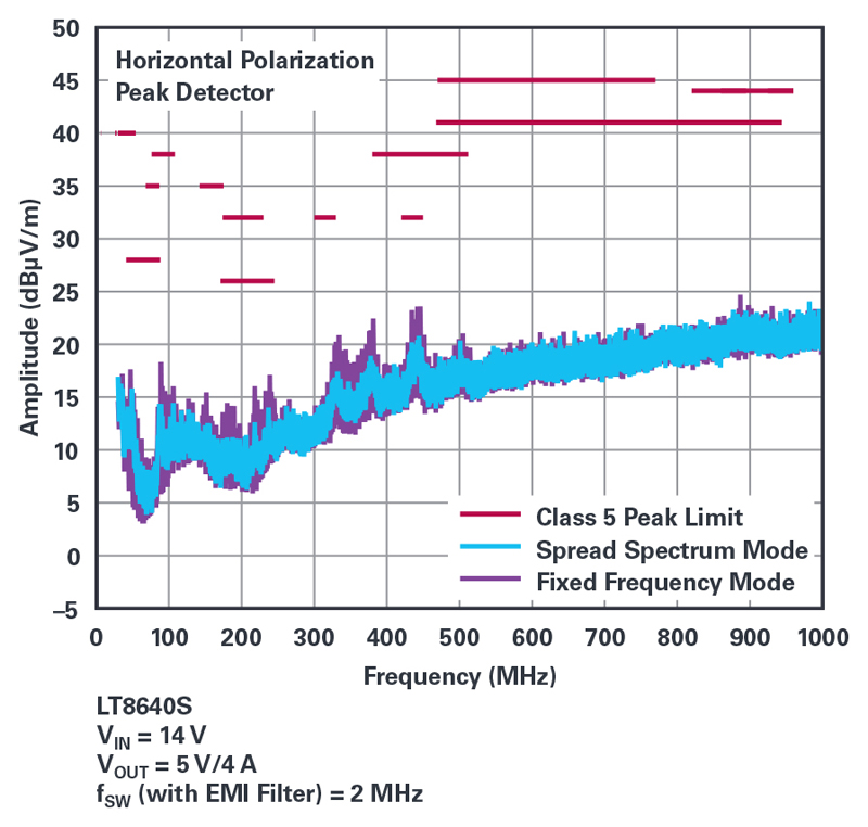
The LT8640S, the second generation of this technology—Silent Switcher 2 (Figure 11) — incorporates the input capacitors in the IC. This ensures maximum noise suppression, eliminating the need to carefully position the input caps in the layout. This feature, of course, also reduces the MLCC requirements. Another feature, spread spectrum frequency modulation, lowers noise peaks by dynamically changing the switching frequency. The combination of these features enables the LT8640S to clear CISPR 25 Class 5 EMC standards for automobiles with ease (Figure 12).
Click image to enlarge
Figure 11. Silent Switcher 2 technology from ADI brings the input caps within the IC, simplifying layout and improving noise suppression
Click image to enlarge
Figure 12. The combination of noise suppression features in a Silent Switcher 2 device, such as the LT8640S, enables easy clearance of CISPR 25 Class 5 peak limits even while reducing input and bypass capacitance
Conclusion
Power by Linear devices from ADI can help reduce MLCC requirements, helping designers ride through the MLCC shortage. Output capacitance requirements are reduced by using high frequency operation while maintaining uncommonly high efficiency. Devices that feature Silent Switcher architecture significantly suppress EMI noise, reducing bypass capacitor requirements. Silent Switcher 2 devices further reduce MLCC needs.