Meeting the safety isolation requirements of power supplies often impacts thermal performance
When designing a switch-mode power supply (SMPS) operating losses and the ability to dissipate heat are critical selection criteria for MOSFETs. The standard TO-220 package is generally good at dissipating heat and the wide range of heatsinks and forced-air cooling options available can easily improve this. Let’s look at the benefits of the TO-220 FullPAK in this kind of situation, and discuss how creepage distances for high voltage SMPS (HV-SMPS) can be enhanced with the latest technology as expressed in devices like this.
Isolation voltage
One critical MOSFET parameter is the isolation voltage. In UL1557 (Standard for Electrically isolated semiconductor devices), production testing is defined to be either the rated isolation voltage for 60 seconds or 120 percent of the rated voltage for 1 second. In the case of FullPAK devices, the rated voltage is 2500 Vrms and all Infineon devices are tested and qualified to this level.
In DC voltage tests, the voltage is gradually raised while monitoring the current flow, allowing a potential breakdown to be detected before it occurs. DC testing is effective in detecting mechanical damage as well as inclusions or areas in the dielectric that have lower resistance. In AC voltage tests, both polarities of voltage are applied. This approach to testing is ideal for products that experience AC voltage during normal operation. As this is closer to normal operating conditions, many manufacturers - including Infineon - use this method of testing.
Thermal issues
Thermal and EMI performance are also important factors. As the tab on standard TO-220 packages is connected to the drain, when mounting to a heatsink a thermally conductive, electrically non-conductive material is sandwiched between the tab and the heatsink. However, this approach can add parasitic capacitance, thus causing EMI issues. To overcome these issues, the TO-220 FullPAK has an overmolded tab that provides isolation with less parasitic capacitance - albeit with slightly lower thermal dissipation.
While the same heatsink can be used for TO-220 and TO-220 FullPAK packages due to their mechanical similarities, a slightly higher heatsink temperature can be expected with the TO-220 FullPAK due to the slightly lower thermal performance. The EMI impact on the design using TO-220 or TO-220 FullPAK mostly depends on the way the device is mounted to the heatsink and how the heatsink is connected electrically. It is generally recommended to connect the heatsink to earth or chassis ground for better EMI performance.
Creepage
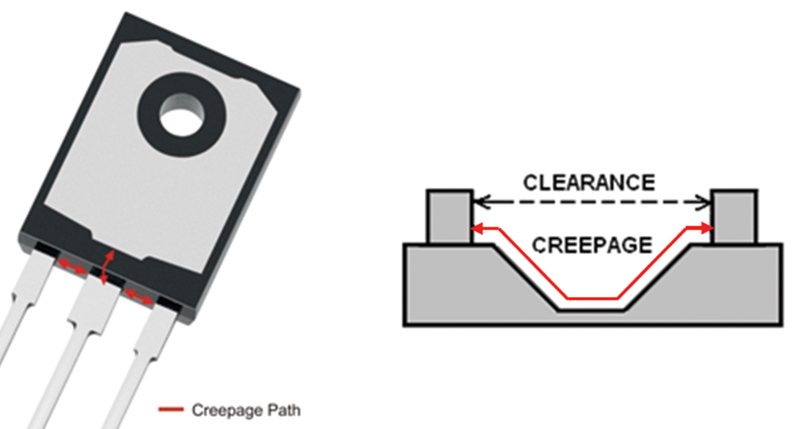
Another important parameter in ACDC SMPS is the creepage distance. Creepage distance is defined as the shortest path between two conductive materials measured along the surface of an isolator that separates the conductors. In practical terms, this is the effective distance between legs of the package when mounted on a PCB. Maintaining a suitable creepage distance avoids the risk of failure due to arcing (see Figure 1).

Click image to enlarge
Figure 1: The creepage distance is the shortest path between two conductors along the surface of an isolator (typically a PCB)
The minimum creepage distance is defined by the safety standards the SMPS is required to meet and depends on working voltage, pollution degree, type of isolation, track resistance of isolation materials (CTI value) and circuit type (primary circuit, etc.). To understand how failures can occur, we can consider a typical LED TV or PC power supply. Similar to many other devices, air vents are included in the external casing to permit airflow, which will assist in cooling the internal components - sometimes with the use of an internal fan to increase the airflow volume.
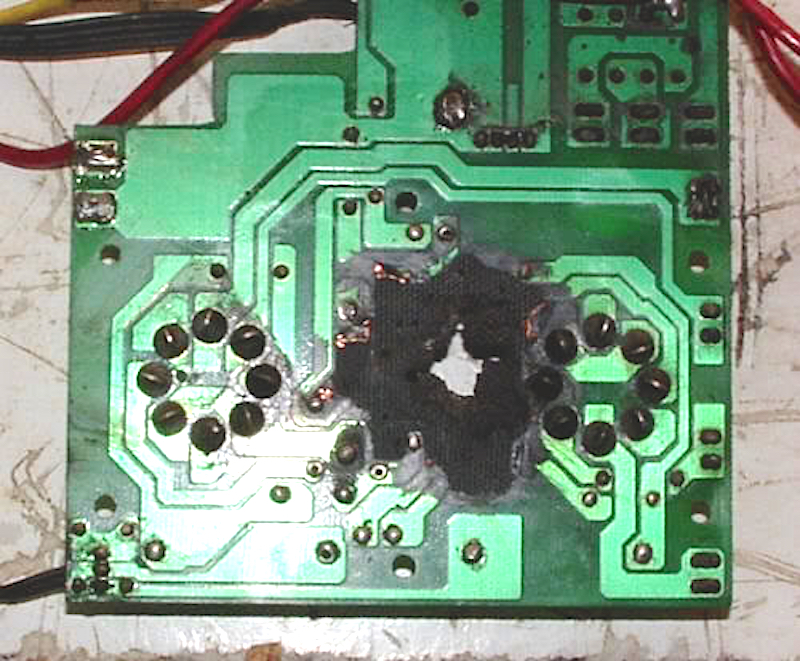
However, air vents make the inside more susceptible to dust particles and other naturally occurring pollutants. These pollutants can gather on the pins of components and reduce the effective creepage distance, allowing arcing between pins. This high-voltage arcing presents a safety hazard and can also, potentially, destroy the MOSFET (see Figure 2).
Click image to enlarge
Figure 2: In vented or open systems conductive pollutants can gather and reduce the effective creepage distance, causing arcing failures
Recognizing this issue, EN60664-1 increases the creepage distance based on the degree of pollution to prevent arcing. For example, the creepage requirement of 2.5 mm in clean or sealed environments increases to 3.5 mm in open frame or dusty environments to allow for the build-up of pollutants.
Increasing the distance
Various techniques exist for increasing the creepage distance. These include sleeving, covering or bending the legs of through-hole devices. In some cases, silicon potting is applied to the legs of the device. Unfortunately, it is very difficult to automate these processes so they add time and cost, as well as another manual operation, to the assembly process.
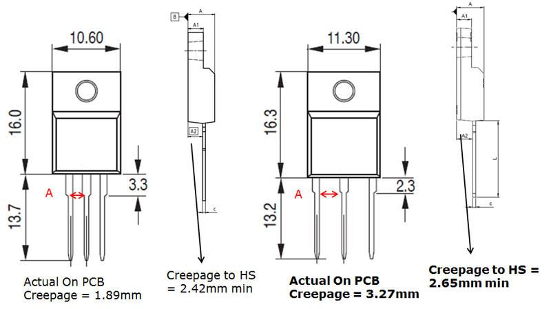
In order to address this issue, Infineon developed a wide-creepage TO-220 FullPAK package within their MOSFET range. Offering increased lead spacing of 4.25 mm between leads, the package is just three percent wider than a standard TO-220 FullPAK package, with the same height and thickness.
The similarities are sufficient to allow standard heatsinks and automated handling tools to be used, yet the increased spacing allows sufficient creepage for polluted environments without the need for additional manual process steps. Thus, the wide creepage MOSFET simplifies the design challenge and saves time, cost and process steps during assembly (see Figure 3).
Click image to enlarge
Figure 3: The TO-220 FullPAK wide creepage package is very similar to standard TO-220 FullPAK, yet increases creepage by 1.38 mm
While the TO-220 FullPAK Wide Creepage improves the distance between the legs, care has to be paid to the distance between the MOSFET leads and the heatsink. This can be achieved relatively easily by ensuring the heatsink is selected or designed with a shape such that it does not get too close to the leads.
The final consideration is the type of mounting used to mechanically connect the MOSFET to the heatsink. One popular modern technique is to use a specially designed isolated clip or isolating foil.
For example, Infineon's CoolMOS CE is an optimized platform designed specifically to address application needs for consumer devices. The CE devices have a large margin between the typical and nominal values of RDS(ON) giving low conduction losses allowing for reduced power consumption and excellent thermal safety margins.
The effort required to design-in CE devices is reduced due to optimized EMI (meeting EN55022B) and an integrated gate resistance (RG) giving improved levels of controllability. CE devices are qualified for standard grade operation and would typically be found in applications such as adapters, PC silver boxes, LED TVs and indoor lighting.
In order to ensure high levels of reliability, CE devices are tested and qualified to levels in excess of the typical application needs. Temperature cycle (TC) testing is based on the expected lifetime of the end product, percentage of usage in ambient temperature, number of on/off cycles of the product and other similar considerations. A typical consumer product would require temperature cycling to be performed for 200 cycles whereas the Infineon CE devices are cycled 500 times as standard during qualification.
The high temperature reverse bias (HTRB) test cycle accounts for the load profile of the application including typical operating load conditions and load duration. Typically, HTRB testing would be performed for 168 hours during qualification yet, again, the CE devices exceed this by a considerable margin, being tested for 500 hours as standard. They offer a range of RDS(ON) values from 190 to 600 mOhm and are identified by a 'W' in the part number - e.g. IPAW60R190CE is a 600V, 190 mOhm TO-220 FullPAK Wide Creepage device.
In summary, the new TO-220 FullPAK Wide Creepage MOSFET package from Infineon builds on the inherent benefits of the TO-220 FullPAK and extends the effective creepage distance to address the pollution-related failure concerns of open frame or vented SMPS. The new TO-220 FullPAK Wide Creepage devices can be retro-fitted to existing designs with relatively simple PCB modifications to allow for the wider lead spacing.
The devices are qualified beyond the needs of most applications and greatly reduce field failures due to creepage related issues when operating in polluted environments. They also reduce the design time and complexity and cost of the assembly process that is associated with conventional TO-220 FullPAK packages.