Selecting High-Voltage Components for Safety and Space Savings
Careful component selection can help utilize space as efficiently as possible while ensuring safety and reliability
The laws of physics can restrict designers’ options in pursuit of miniaturization when high operating voltages are involved. Careful component selection can help utilize space as efficiently as possible while ensuring safety and reliability.
Designing equipment to operate at voltages above a few hundred volts places constraints on engineers that run counter to the usual objective – which is to pack as much functionality and the best possible performance within a small form factor often defined by industry standards or market expectations.
Instead, designing for high-voltage operation imposes minimum requirements on physical dimensions to ensure safety. “Normal” dielectric material properties can change when a high voltage is applied, not be taken for granted, causing insulators to support arcing between electrodes, or allow an electrical charge to pass instead of being blocked. Arcing can permanently damage equipment or components, while insulation breakdown can present a risk of electric shock for users.
Safety and Size Constraints
It is vital to select materials and components that not only have a suitable voltage rating – typically the rated voltage should be at least twice the maximum nominal applied voltage – but also to ensure appropriate creepage and clearance distances.
· Creepage refers to the tendency for an electric field to spread out across the surface of a dielectric, between two electrodes at different potentials. The stronger the field, measured in kilovolts per millimeter (kV/mm), the greater the creepage distance needed to prevent arcing between the electrodes.
· Clearance is the minimum distance required to prevent arcing between two electrodes at different potentials, separated only by air.
From these descriptions, it should be clear that the term “electrodes” may refer to various types of conductors, such as component terminals, PCB traces, connector pins, or any combination of these that may be sitting at different voltages while in close proximity to each other. The dielectric may be the outer packaging of a component, the surface of a PCB, or insulating components of a connector.
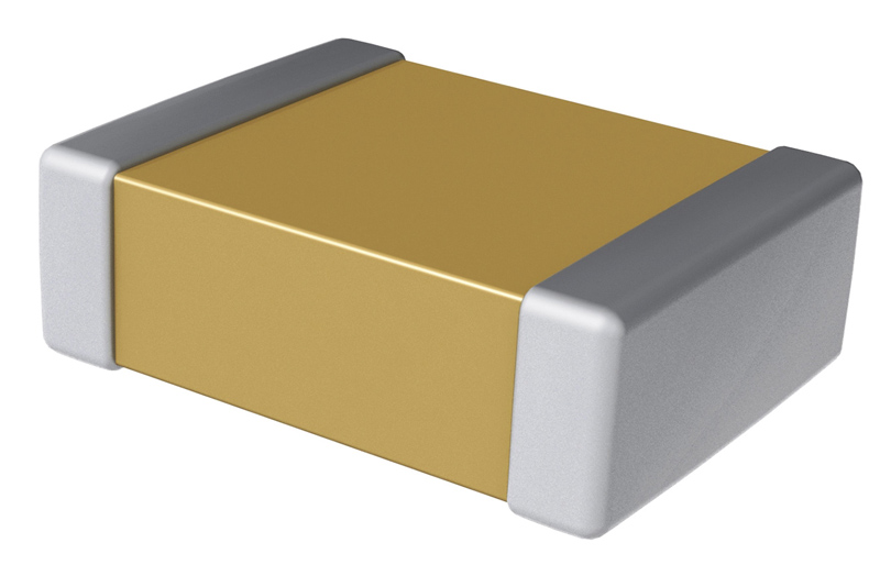
In the case of a multi-layer ceramic capacitor (MLCC), for example, a working voltage as low as about 300V can establish an electric field strong enough for the applied energy to arc across the surface of a poorly selected component, instead of passing through the capacitor. This can result in the breakdown of the capacitor’s dielectric, causing a short circuit that ultimately leads to device failure.
While it would be convenient to be able to stipulate minimum creepage and clearance distances according to the applied voltage, in practice many other variables such as environmental conditions, the risks posed to users or equipment, and industry- or market-specific safety standards require designers to consider each application on its own merits. For example, high environmental humidity, or contamination of the dielectric surface can promote ionization, resulting in increased likelihood of arcing. To prevent contamination, a protective glass-based coating may be applied to some types of components, such as resistors or chip capacitors, or a conformal coating may be applied to a PCB.
AVX’s SXP molded, radial, multilayer capacitors show how high-voltage passive components are designed with extended creepage and clearance distances. The largest member of the family, the SXP4, is available with capacitance values from 100pF to 2700pF, in a 22.4mm x 16.3mm x 5.84mm case size with lead spacing of 19.8 mm. This spacing is about the length of a standard paper clip.
Advanced component technologies can help ensure superior creepage and clearance within smaller overall dimensions. An example is KEMET’s ArcShield technology for. ArcShield capacitors like the C1210W683KDRACTU X7R MLCC incorporate a shield electrode inside the component, which effectively reduces the electric field strength across the component surface thereby preventing conditions that can cause arcing. This technology enables chip capacitors in case sizes as small as 0603 to support operating voltages of up to 1kV.
Cables and Connectors
When considering the creepage and clearance distances between conductors such as PCB traces, interconnects, or cable terminations, the system designer, must take responsibility for ensuring adequate physical separation. When it comes to connectors, particular attention must be paid to select suitable parts, whether these are standard off-the-shelf or custom items. In either case, it is the connector manufacturer, not the system designer, who determines and defines the voltage rating of the connector for different applications and situations.
High-voltage connectors are typically designed for specific industries and applications. A vendor may, for example, describe a part as being "rated to 2000V DC for medical applications, per standard IEC 60601". This gives product designers a clear indication as to the suitability of the connector for their intended purpose.
On the other hand, the shape and physical features of some high-voltage interconnects can sometimes give a clear indication of their intended purpose. Cable assemblies for railway roofline systems, which connect the high-voltage overhead cables to transformers on-board the rolling stock, provide one example. TE Connectivity HVTT and HVTE cable assemblies are rated to 15/25 kV and feature AC-withstand voltage of 50/90kV and impulse-withstand voltage to 125/175kV. The size and shape of these assemblies (Figure 2), with their smooth surfaces and textures, are engineered not only to avoid high concentrations of electric field strength but also to maximize discharge. There design guards against arcing when the train is stationary or moving slowly in heavy rain. It also helps to prevent the build-up of surface contaminants due to corrosion. Their large size, with diameters of 90 to 135mm, combined with careful design, give creepage distances of 650mm to 1000mm.
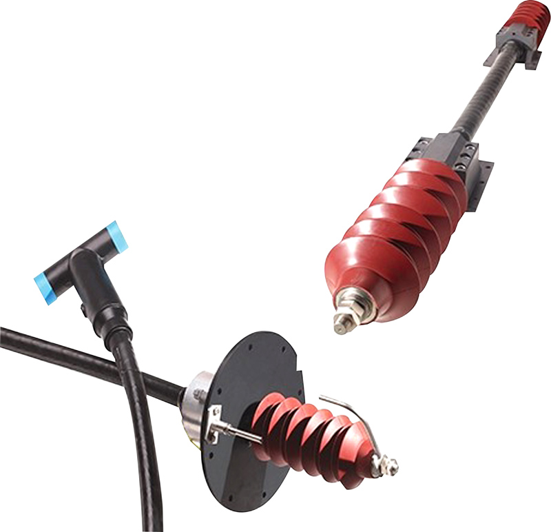
Click image to enlarge
Figure 2: The external shape of some high-voltage components serves to enhance safety and reliability.
High-Voltage Power Control
In some applications, very high voltages are needed purely to cause an excitation effect: some examples include X-ray tube drivers, millimeter-wave generators, or electron-beam generators for scientific microscopy equipment or for electron lithography as used in producing semiconductor mask sets. Although applied voltages can be extremely high, current flow may be relatively low.
High-power systems, on the other hand, can benefit from lower energy losses and self-heating (governed by I2R), as well as reduced conductor thicknesses, by stepping up to a high voltage to allow a corresponding reduction in current. Applications can range from domestic appliances to variable-frequency industrial drives, or high-voltage DC power distribution.
For a circuit such as a single-ended parallel resonant converter, as typically used in stove-top induction heating systems or microwave ovens, a high-voltage IGBT such as the Infineon IHW30N160R2 has a high breakdown voltage of 1600V and can handle up to 30A continuous collector current. It is capable of operating at a switching frequency of up to 60kHz, which significantly extends the scope for designers to use smaller magnetic and passive components. Industry-standard power packages are easy for system designers to use and deliver known performance in terms of current capability and creepage and clearance distances for high-voltage applications. The IHW30N160R2 comes in a TO-247 with leads a little over 1mm wide, and lead separation of about 5mm.
While IGBTs like this Infineon device are typically preferred for power circuits operating at higher voltage, higher current, and lower switching frequencies, power MOSFETs tend to deliver better performance at combinations of lower voltage and lower current, with higher switching frequency. With the arrival in the market of commercial silicon carbide (SiC) MOSFETs, engineers can now explore more ways to achieve their desired combination of high-voltage capability, high switching speeds that allow smaller external components, and low conduction losses. Also, SiC delivers the extra advantage of a higher maximum operating temperature, allowing more rugged and reliable circuits with reduced reliance on thermal management such as heatsinks or cooling fans.
These performance advantages of SiC devices, over conventional silicon MOSFETs, stem from their wide-bandgap characteristic. In other words, greater excitation is needed to raise electrons into the conduction band: about 3.2eV, compared to about 1.1eV for silicon. Because higher energy is required, the breakdown voltage is significantly higher compared to the conventional silicon die on the same scale. Hence device designers can create SiC MOSFETs in established and widely used voltage ratings – such as 1200V or 1700V for high-voltage applications – with greater freedom to optimize the gate, drain and source regions for lower RDS(ON).
SiC devices can carry high current with low losses, and high thermal conductivity allows greater system power densities. The Cree C2M family of 1200V and 1700V SiC MOSFETs shows how this emerging technology is poised to raise the bar in high-voltage power-systems design. Housed in the industry-standard TO-247 package, the 1.2kV C2M0160120D can handle drain current up to 17.7A yet has RDS(ON) of just 160mΩ. Cree claims that its SiC MOSFETs enable three times the power density of conventional silicon IGBTs, with only 20% of the losses. SiC power MOSFETs like the C2M series are an exciting prospect for use in energy-conscious applications such as solar inverters and uninterruptible power supplies (UPS), as well as high-voltage DC/DC converters, high-performance industrial motor drives, and general switched-mode power supplies (SMPS).
Conclusion
Designing circuitry for applied voltages of hundreds or even thousands of volts requires understanding aspects of material properties and electric-field behavior that do not apply at lower voltages. Although, on the one hand, high-voltage/low-current power distribution can allow conductors of smaller cross-section than would be required at lower voltages, demand for larger separation distances can hamper designers’ desires to minimize circuit size and increase power density. Special technologies like KEMET’s ArcShield can help meet creepage and clearance within standard chip-component form factors, while high-voltage know-how is often evident in the shape, size, and environmental protection designed into parts such as connectors. In the world of power semiconductors, SiC technology enables more favorable trade-offs between size and performance.
At such voltages, both the selection and application of components must be carefully considered to ensure functional integrity, reliability, and safety.
Mouser Electronics


