Selecting the Right MOSFET for Power Factor Correction Applications
Device choice impacts a PFC circuit on the line current and its harmonics
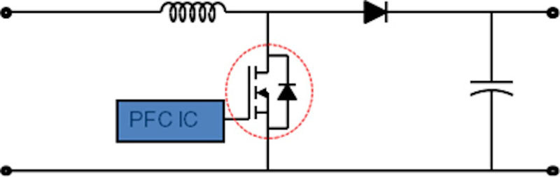
Figure 1: PFC schematic
Power factor is the ratio of the real power (P = Watts) to the apparent power (VA = Volt Ampere); the goal is to achieve a power factor as close to 1 as possible. A load with a lower power factor draws more reactive current than a load with a higher power factor for the exact same output power. The higher current increases the energy lost within the system, and for utility companies, results in excessive wasted power in transmission. For this reason, a power factor correction (PFC) circuit block, shown in Figure 1, is an important, and often mandatory, sub-system of any power supply with an output power of 75 W or more (per EN61000-3-2). A PFC circuit block is used to align the input line current with the AC voltage waveforms, and in most cases boosts the output voltage to a common 400 VDC. Figure 2 shows the impact of a PFC circuit on the line current and its harmonics.
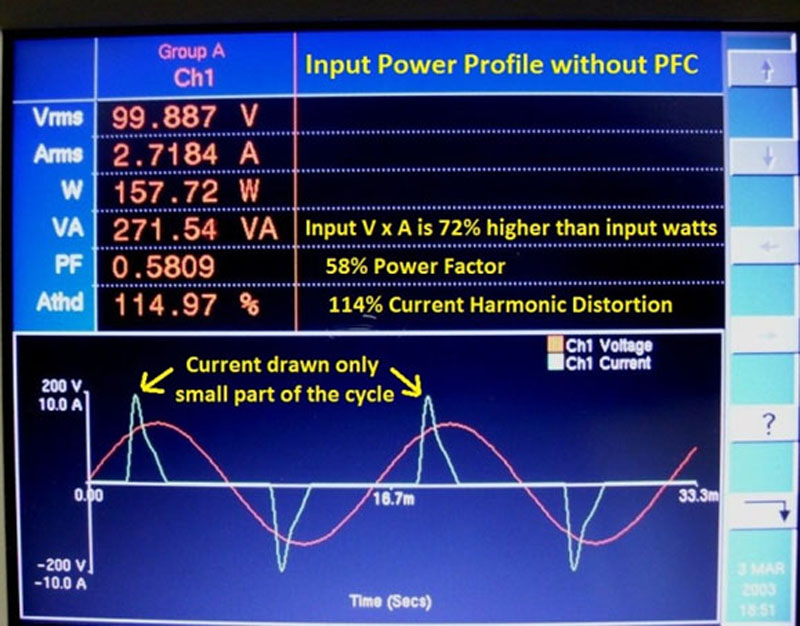
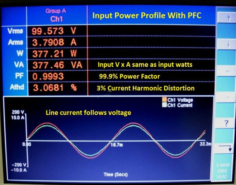
In Figure 2A, current is drawn from the AC supply only for a short duration of the cycle. This results in a poor power factor and excessive harmonics of 115%. While the system draws only 158 W of usable power, 272 Volt-Amperes are circulated in the transmission system to deliver it. Figure 2B shows the benefits of implementing PFC using the same input power profile. With a power factor of 99.9%, harmonics are down to 3%. Current is drawn from the AC line throughout the cycle and no excessive Volt-Amperes are wasted.
It should be noted that PFC and harmonic current reduction are not synonymous. For example, in a highly inductive load, the current may be a perfect sinusoid lagging the voltage. It will then have a poor power factor and high reactive power without any harmonics at all. Whereas a distorted waveform, rich in harmonic currents, usually has all the undesirable features. The PFC circuit corrects more than just the power factor; it reduces the harmonics. Today, there are different standards specifying the quality of power drawn by electronic equipment. EN61000-3-2 requires harmonic current reduction on all systems with input power of > 75W. The 80 Plus power supply certification requires a power factor of 0.9 or more. In a PFC circuit, the MOSFET is responsible for approximately 20% of all losses. By choosing the correct device, PFC efficiency can be greatly increased. One way to select the right MOSFET for a PFC circuit is by using an application-specific Figure of Merit (FOM) that is focused on minimizing total losses in the device. While it includes on-resistance (RDS(on)) for conduction losses and gate charge (Q(sub>g) for switching losses, the FOM is not a simple product of the two. In order to account for switching losses, a portion of the device's Qgs and Qgd, along with its output capacitance (Coss), are used. The four stages of a standard AC/DC power supply • Input • PFC front end • Converter • Secondary To meet 80 Plus Gold efficiency standards, the combined loss for all stages is ~ 12% of the rated output power. The PFC MOSFET alone should be limited to around 2% of the total output power or the package power limit, whichever is lower. The maximum power loss limits of "TO" packages: • PowerPAK SO-8L (5x6): 5W • PowerPAK 8x8: 7W • TO-220 / TO-220F: 10W • TO-247: 20W • Super TO-247 / Tmax: 25W So, the maximum package power limits that consist of both conduction and switching losses should not exceed the above levels. Conduction loss is a simple I2*R calculation that takes into account the RDS(on) of the device as well as its temperature coefficient. The switching losses need to take into account not only Qg, Qgd, and Qgs, but also Qoss, which is an integral function of Coss. The traditional FOM, RDS(on) (typ) * Qg (typ), does not take into account the Coss/Qoss of the device, which is a very important loss, especially at light loads where switching losses trump conduction losses. This component of the switching loss is incurred both ways, as Coss is charged when the device turns off and discharged when it is turned on, and has to be taken into account in the design. The larger the Coss/Qoss, the larger the switching losses. In addition, the Qoss loss is fixed and independent of load, as can be seen by the standard equation Poss = ½ CV2 x Fsw, where Fsw is the switching frequency. In universal input power supplies, the PFC MOSFET is always subjected to the bulk DC bus voltage of 380 VDC to 400 VDC. As a result, the output switching loss can be a significant portion of the total losses. The Coss of a high-voltage MOSFET (HVM) varies considerably with the applied VDS. This variation is much wider for high-voltage Super Junction power MOSFET than for planar types. To account for the non-linearity of the output capacitor, Poss = ½ Coer x V2 x Fsw may be used as the loss equation. Coer is the effective capacitance that has the same stored energy and same losses as the integrated Coss of the MOSFET, and is provided in the datasheets. So, the new FOM will now look like Rds(on) (typ) * (Qswitch (typ) + Qoss), where Qswitch is a combination of Qgd and Qgs. As an example, we'll use a TO-220 / TO-220F device with a maximum package power loss of 8W, and contribute 4W to conduction losses and 4W to switching losses. The Coss/Qoss losses would contribute to approximately 20% of the overall package loss, or 40% of the total switching losses, which is a large loss that is not taken into account with the standard FOM equation.
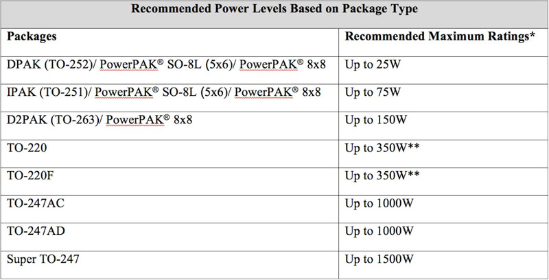
With many package options available, Table 1 lists the recommended maximum power rating for the different package offerings. Note that there will be a range of devices available in each package, which is why the same package may be recommended over a wide range of output power. To realize the maximum possible power dissipation of SMT packages like PowerPAK SO-8L (5x6) and PowerPAK 8x8 it is necessary to maintain PCB temperature at required application needs under worst case conditions. The Recommended Maximum Ratings are therefore limited by system thermal considerations rather than the package loss. Vishay