Separating and Mitigating Conducted Emissions
A practical method for separating common-mode and differential-mode emissions in conducted emissions testing
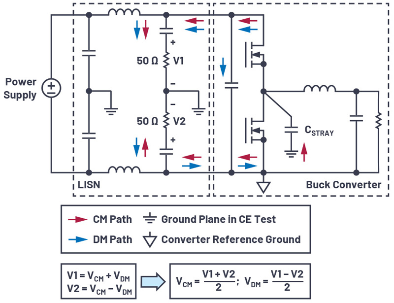
Figure 1. The CM noise path and DM noise path in a buck converter
EMI from switching regulators is broken down into radiated and conducted emissions (CE). This article focuses on conducted emissions, which can be further classified into two categories: common-mode (CM) noise and differential-mode (DM) noise. Why the CM-DM distinction? EMI mitigation techniques tha tare effective for CM noise are not necessarily effective for DM noise,andviceversa, so identifying the source of conducted emissions can save time and money in suppressing it. This article presents a practical method of separating CM emissions and DM emissions from the total conducted emissions for an LTC7818 controlled switching regulator. Knowing where the CM noise and DM noiseappear in the CE spectrum enables power supply designers to effectively apply EMI suppression techniques, which saves design time and BOM costs in th elongrun.
Figure 1 shows the CM noise and DM noise paths for a typical buck converter. DM noise is produced between the supply line and the return line, while CM noise is produced between the supply lines and the ground plane (such as a copper test table) via stray capacitance, CSTRAY. The LISN for CE measurement is placed between the power supply and buck converter. The LISN itself can not be usedf or direct measurement of CM and DM noise, but it does measure supply and return supply line noise—V1 and V2 in Figure1,respectively.These voltages are measured across 50 Ω resistors. From the definition of CM and DM noise, shown in Figure1, V1 and V2 can be expressed by the sum and difference of the CMvoltage (VCM) and DM voltage (VDM), respectively. This allows us t calculate VCM from the average of V1 and V2, and VDM as half of the difference between V1 andV 2.
Measuring CM Noise and DM Noise
A T type power combiner is a passive device that combines two input signals to a single port output. A 0°combiner produces a vector sum of the input signals at the output port and a 180° combiner produces a vector difference of input signals.1 Therefore, a 0° combiner can be used to produce VCM and a 180° combiner to produceVDM.
ZFSC-2-1W+ (0°) and ZFSCJ-2-1+ (180°) combiners from Mini-Circuits, were used to measure VCM and VDM from 1MHz to 108MHz. For these devices, measurement error increases for frequencies below 1MHz. For lower frequency measurements, use different combiners, such as ZMSC-2-1+ (0°) and ZMSCJ-2-2 (180°).
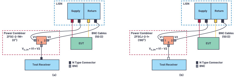
The diagram of the test setup is shown in Figure 2. The power combiner is added to the standard CE test setup. The outputs of the LISN for the supply line and return line are connected to Input Port 1 and Input Port 2 of the combiner, respectively. For the 0° combiner, the output voltage is VS_CM = V1 + V2; for the 180° combiner, the output voltage is VS_DM = V1 – V2.
Click image to enlarge
Figure 2. Experimental setup for measuring (a) VCM and (b) VDM
The output signals of combiners VS_CM and VS_DM must be processed in the test receiver to produce VCM and VDM. First, the power combiners have specified insertion losses compensated in the receiver. Second, since VCM=0.5VS_CM and VDM=0.5VS_DM, the test receiver subtracts an additional 6 dBµV from the received signal. After compensating for these two factors, the measured CM noise and DM noise are read in the testreceiver.
Experimental Verification of CM Noise and DM Noise Measuring
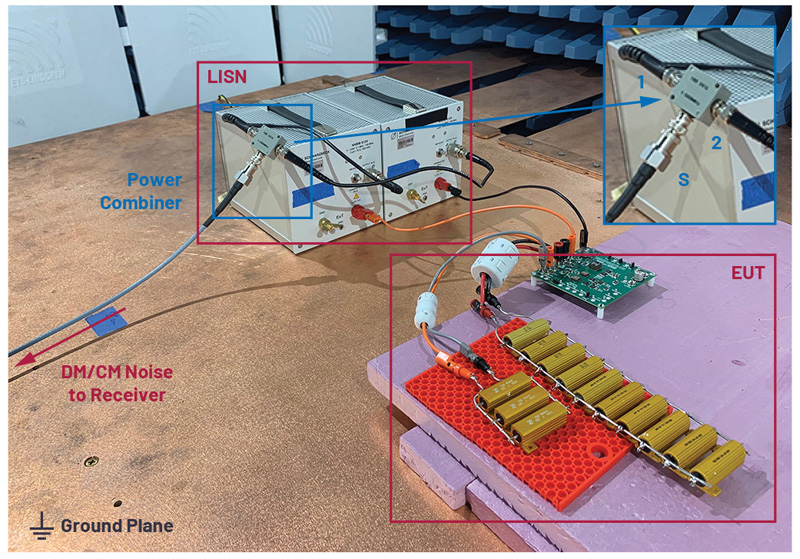
A standard demo board with dual buck converters is used to verify this method. The switching frequency of the demo board is 2.2MHz, while VIN=12V,VOUT1=3.3V, IOUT1 = 10 A, VOUT2 = 5 V, and IOUT2 = 10 A. Figure 3 shows the test setup in the EMI chamber.
Click image to enlarge
Figure 3. Test setup for measuring CM noise and DM noise
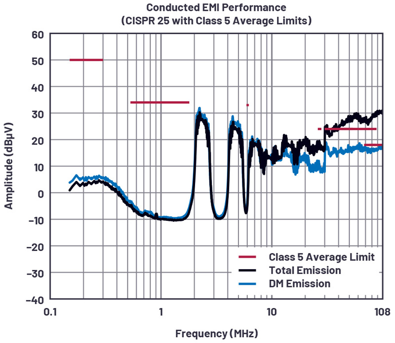
Figure 4 and Figure 5 illustrate the test results. In Figure 4, the higher EMI curve shows the total voltagemethod CE measured with the standard CISPR25 setup, while the lower emissions curve shows the separated CM noise measured by addingthe 0° combiner. In Figure 5, the higher emissions curve shows the total CE, while the lower EMI curve shows the separated DM noise measured by adding the 180° combiner. These test results comply with theoretical analysis, suggesting that DM noise dominates the noise at a lower frequency range,while CM noise dominates at the higher frequency range.

Click image to enlarge
Figure 4. Measured CM noise vs. total noise
Click image to enlarge
Figure 5. Measured DM noise vs. total noise
Adjusted Demo Board Passes CISPR 25 Class 5
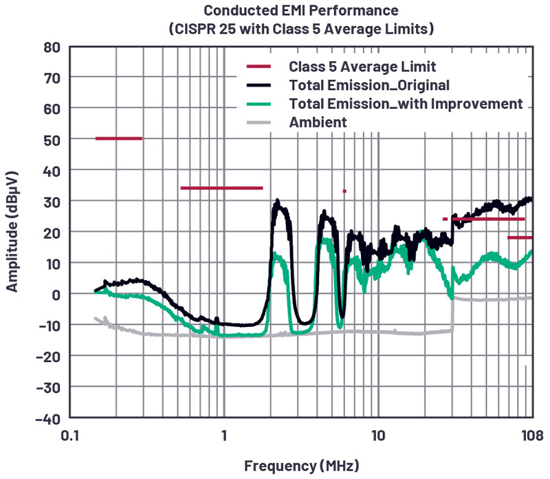
According to the measured results, the total noise emission exceeds the limit of CISPR 25 Class 5 at the range of 30 MHz to 108 MHz. By separating the CM and DM noise measurements, it appears that the high conducted emissions at this range are caused by CM noise. It makes little sense to add or enhance the DM EMI filter or otherwise reduce the input ripple, as these mitigation techniques would not reduce the problematic CM noise at this range.
Therefore, methods specifically addressing CM noise are implemented on this demo board. One source of CM noise is high dV/dt signals in the switching circuit. Reducing dV/dt by increasing the gate resistance can decrease the noise level. As previously mentioned, CM noise passes through the LISN via the stray capacitance CSTRAY. The smaller the CSTRAY, the lower the CM noise detected in LISN. To reduce CSTRAY, the copper area of the switch node cuts down on this demo board. Furthermore, a CM MEMI filter is added at the input of the converter to obtain high CM impedance, therefore reducing the CM noise into the LISN. By implementing these methods, the noise at 30 MHz to 108 MHz is reduced enough for compliance with CISPR 25 Class 5, as shown in Figure 6.
Click image to enlarge
Figure 6. Total noise with improvement

.jpg)