Provides a Compact and Efficient AC/DC Supply
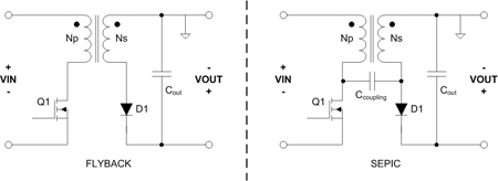
Most isolated low-power AC/DC power supplies tend to use the flyback topology due to its simplicity and decent efficiency. Removing the isolation requirement allows other topologies to be used, such as the buck or SEPIC. However, the buck topology requires driving a high-side switch, which often leads to excess circuitry and wasted power. The flyback is still an option, but with no isolation requirement, the coupled-inductor SEPIC topology can reduce the size and improve efficiency compared to a flyback. Figure 1 shows how the power stages of a flyback and couple-inductor SEPIC are very similar. In fact, the only difference between the two schematics is the addition of the coupling capacitor (Ccoupling). In both topologies, while the MOSFET (Q1) is on, the core of the transformer/coupled-inductor is energized. While the MOSFET is off, the energy in the magnetic device is directed to the output through D1. At the instant when Q1 is turned off, any residual energy remaining in leakage inductances must go somewhere. In the flyback, a clamping circuit is usually added to the MOSFET to prevent this leakage energy from causing an over-voltage stress on the device. In the coupled-inductor SEPIC, the leakage energy is redirected to the output through the coupling capacitor, clamping the voltage on the MOSFET. Redirecting the leakage energy reduces power loss and can improve the supply's efficiency by approximately two percent. The coupling capacitor also clamps the reverse voltage on the diode and significantly reduces ringing that can cause electromagnetic interference (EMI) problems in flyback converters.
The DC conversion ratio is the same for the flyback and coupled-inductor SEPIC. The resulting equations defining the duty cycle as a function of input and output voltage are given by equation 1 for continuous operation and by Equation 2 for discontinuous operation. In a flyback, the number of primary and secondary turns can be adjusted and optimized for any given input range and output voltage. By contrast, the ratio of primary turns to secondary turns in a SEPIC must be 1:1. In applications with large input voltage to output voltage ratios, this creates design challenges and limits the flexibility of the SEPIC.
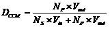
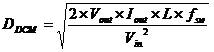
Figure 2 shows the schematic of a 5V/1.25W SEPIC converter that is powered from an 115VAC input. The rectified AC line voltage produces an input voltage of approximately 160VDC. For continuous operation, the SEPIC converter operates with a duty cycle of around three percent. For discontinuous operation, the duty cycle is even less. At these very small duty cycles the converter becomes sensitive to perturbations in on-time. By lowering the switching frequency, the on-time is increased and this noise sensitivity is reduced. Also, by using a large inductance, continuous operation and a wider duty cycle is guaranteed over a broader load range. In this example, a 40kHz switching frequency was selected, which is above the audible range, but low enough to keep the on-time at nearly 1?s during normal operation.
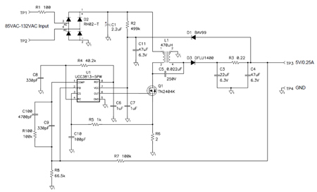
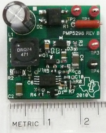
By carefully selecting the switching frequency and inductance, a physically small circuit can be designed. The coupled-inductor is one of the largest components. For this example, a dual-winding, surface mount, drum core inductor is chosen. These types of coupled-inductors are compact, cost-effective, and readily available from multiple vendors. When choosing a coupled inductor, be careful not exceed the maximum saturation current rating of the device. Also, pay particular attention to the core loss, which can become excessive at lower frequencies. Most vendors do a good job of providing core loss information in their datasheets. Selecting the proper controller is another key to reducing the amount of circuitry and size of the design. Most off-line pulse width modulation (PWM) controllers are intended to be used with an optocoupler and secondary-side regulation. Hence, they do not contain a reference or error-amplifier. Finding a controller with both of these features may require some hunting through IC vendor websites. In this design, the low output voltage places an additional constraint on the controller that it must operate with less than 5V on VCC. In our test we used the UCC3813-5 because it meets all of these requirements. With a high input voltage and low output power, the current stress on the MOSFET (Q1) is fairly benign. In this case it is around 25mArms. We used a 4-Ohm, 240V device in a SOT23 package because of its small size. Likewise, ceramic capacitors are used in the output filter to keep the design as compact as possible. The resulting design is able to fit into a small one-inch by one-inch single-sided PCB, as shown in the photograph of Figure 3.
In addition to being physically small, this circuit is also fairly efficient for such a large input-to-output conversion ratio. With a 150VDC input and 200mA being supplied to the output, this supply has an efficiency of 60 percent. Also, because the SEPIC tolerates wide input ranges well, this supply can operate down to 20VDC on the input. This allows this circuit to ride through brown-out conditions with very little input capacitance. It might be tempting to extend this design to the universal AC input range of 85VAC to 265VAC. However, at 265VAC input, the rectified input to the converter is approximately 375VDC. At this input voltage, the duty cycle will be less than 1.5 percent, making it more noise sensitive and difficult to control. Moreover, the higher input voltage increases the overall size of the circuit. The coupled inductor is larger and may need to be custom designed. Additionally, the MOSFET would need to be rated for more than 400V, which means it will also be in a larger package. For this wider input range, a flyback normally makes more sense. In conclusion, the SEPIC converter can provide a very compact solution for low-power bias supplies when isolation is not required. Using standard off-the-shelf drum core inductors is key to reducing the size. The design example given can be easily modified for other output voltages ranging from 3.3V to 15V with good efficiency. For more information about this and other power solutions, visit www.ti.com/power-ca www.ti.com


