Server / Telecom - Si and WBG solutions: Part 3 of 4 Editorial Series Sponsored by Infineon; Towards Efficient, Reliable, and Cost-Effective Power Supply Units for 5G Telecom Rectifiers Applications Using Wide-Bandgap Semiconductors

How to meet the design challenges of modern telecom SMPS through SiC and HV/MV GaN technologies
Figure 1: Key features required for AC-DC SMPS in the latest generation of telecom applications
The 5G spectrum has been released in several countries worldwide and already in commercial use. 5G is accelerating and promises to change our lives thanks to large bandwidth, massive connection, and ultra-low latency.
On top of this network evolution, we need to consider the advancements in the so-called mobile edge computing (MEC) area as well. It will support application fields with ultra-low latency requirements, such as Internet of Things (IoT) services, autonomous driving, or smart manufacturing. In order to get a minimal delay in the communication, the servers will be moved more and more from the traditional data center/cloud all the way to the radio access network by contributing to an increase in the total telecom power consumption.
Even if the 5G network’s growing significance is inevitable, the different spectrums will co-exist for some time. This co-existence of old and new spectrums at the first step requires the optimization of the cabinets. But simply adding new power supplies into the existing cabinet is not the solution. This approach would create a proliferation of new cabinets, which is definitely unwanted due to space constraints and exceptionally high ground rental fees.
Thus, telecom sites must be accurately re-designed, starting from the power supply units (PSUs), which will be replaced by new ones with higher output power and typically higher efficiency and smaller form factor.
This article presents the appropriate design choices for telecom switched-mode power supply (SMPS) based on the requirements set by the 5G technology. We explain the role of wide-bandgap technologies in a telecom SMPS system’s reliability and performance by considering typical design SMPS aspects and trade-offs to simultaneously achieve high efficiency and high power density.
Trends and challenges in modern telecom 5G power architectures
Small- and micro-sites gain growing importance and become key structures in the 5G era. The harsh environment where they typically work makes especially those systems susceptible to the power supply reliability. Similar requirements can also affect the MEC systems, especially when these are located in outdoor environments.
In general, any new site construction cost becomes higher and higher, but the most crucial one is going to be the site maintenance cost. In fact, the site maintenance cost accounts today for 2 percent to 5 percent of the total revenue of any mobile network operator (MNO). On the other hand, due to the proliferation of small-, micro-, and macro-cell, we can expect an immediate increase of that percentage. Due to this, it is easy to predict that system reliability, starting from the SMPS one, is a “must” to safeguard the financial health of the MNOs, especially the smallest ones.
From the trends and challenges mentioned above, we can derive three key general requirements for the 5G infrastructure:
• High efficiency. Achieving high efficiency is the best way to reduce heat dissipation (due to high power consumption compared to 4G) and operational expenses (OPEX).
• Re-use of existing infrastructure. Same cabinets, cablings, and connections; power distribution and system footprints must not change. This leads to significant capital expenses (CAPEX) reduction.
• Simplified operational/maintenance (O/M) costs and high reliability. Due to the pinpoint deployment, O/M costs heavily affect the total OPEX.
Power supplies requirements in 5G telecom base stations
The requirements mentioned above for 5G infrastructure translate into some key features required for AC-DC SMPS in the latest generation of telecom applications. Figure 1 below summarizes these features.
Power density is a consequence of higher power requirements in the same form factor as previous SMPS, allowing the re-use of the old cabinets. Also, lower height is necessary when the PSU is assembled close to radio equipment, as in small-cell applications. Modularity typically helps power density, economies of scale and reduces time to market.
The increasing use of outdoor installations is especially valid for new active antenna systems (AAS) base transceiver stations (BTS). This allows removing the cabinet at the tower’s foot by installing power and equipment onto the tower or on the rooftop to reduce the site rental cost. This also applies to small cell applications due to the increasing requirement of AC-DC PSU integrated with radio equipment, especially in 5G mmWave systems
The required flatness of the SMPS efficiency curve is a consequence of the more uneven 5G data traffic than the 3G/4G communication. This is also a sign of a general higher utilization factor of the PSU, making the full load efficiency as important as the mid load one. Moreover, minimizing the heat generated at full load is also a high power density enabler since less heatsink volume is needed in the worst operating condition from the thermal point of view. In conclusion, 30-100 percent is the load range in the focus of modern 5G telecom rectifiers. Of course, high peak efficiency (up to 98.5 percent) is crucial to reduce OPEX, especially in installations in places with high kWh costs, like in MEC systems.
The O/M cost reduction has apparent impacts on the SMPS reliability, with a required lifetime ≥ 10 years and MTBF >1000000 hours (according to Telcordia SR-332 standard).
The role of wide-bandgap (WBG) technologies in telecom 5G SMPS: performance and reliability aspects
All the trends and requirements mentioned above significantly influence the design of power supplies for telecom 5G applications, also historically known as “telecom rectifiers.” In the following, we explain how WBG technologies, such as CoolSiC™ MOSFETs and medium voltage (MV) and high voltage (HV) CoolGaN™ e-mode HEMTs, contribute to fulfilling the key 5G SMPS requirements.
Performance for telecom rectifiers
For this purpose, the first important target is to achieve high efficiency and high power density simultaneously. This analysis refers to the typical specification of a telecom rectifier for macro base stations (Table 1).
Click image to enlarge
Table 1: Typical specifications of a telecom rectifier for macro base stations
Our analysis follows the typical design considerations in an SMPS, starting with device selection for the PFC, then for the high-voltage (HV) isolated DC-DC converter, and finally, the synchronous rectification on the secondary side.
The best way to combine high efficiency with high power density in state-of-the-art telecom rectifiers is to use a bridgeless PFC stage such as a totem-pole and a resonant HV DC-DC stage such as an LLC converter with FB or center tap synchronous rectification on the secondary side.
PFC stage
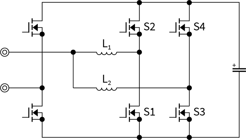
The continuous conduction mode (CCM) totem-pole is the most popular topology in the bridgeless PFC stage (see Figure 2).
Click image to enlarge
Figure 2: CCM totem-pole based on HV SiC / GaN technologies
Click image to enlarge
Figure 3: TCM totem-pole based on Si / SiC / GaN technologies
It consists of:
· A high-frequency path (S1 and S2 devices), where only WBG devices can be used because they can survive the continuous operation in hard commutation typical of this topology. [1],[2]
· A low-frequency bridge leg (S3 and S4 devices), where CoolMOS™ devices with very low RDS(on) represent the ideal choice.
Si Superjunction (SJ) devices like CoolMOS™ can be used in the high switching frequency section of the totem-pole PFC only when triangular current mode (TCM) control is applied with a variable switching frequency, like in Figure 3. Higher components count and control complexity make this topology less convenient compared to the WBG-based CCM.
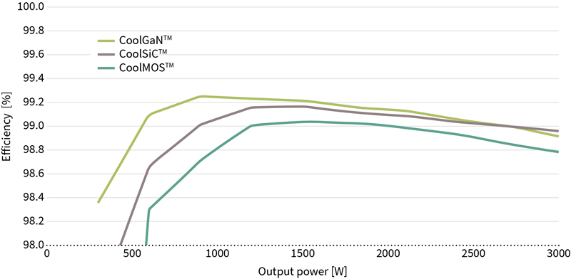
Figure 4 below shows the calculated efficiency of a 3 kW totem-pole PFC stage of a telecom rectifier using CoolGaN™, CoolSiC™ (both in CCM), and CoolMOS™ SJ (in TCM) in the same range of RDS(on) and running at a comparable switching frequency. The rectifier is supposed to work at the nominal conditions (VIN = 230 VAC and TAMB = 40 °C)
Click image to enlarge
Figure 4: Calculated efficiency of a 3 kW totem-pole PFC stage of a telecom rectifier using CoolGaN™, CoolSiC™ (both in CCM), and CoolMOS™ SJ (in TCM) in the same range of RDS(on) and running at a comparable switching frequency
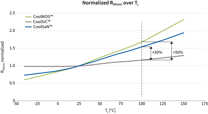
This plot shows that all three technologies allow exceeding 99 percent efficiency at 50 percent load. CoolGaN™ technology shows significant benefits compared to SiC and Si SJ below 30 percent load. This is due to the best figures of merit (FOM) RDS(on)*Qrr, RDS(on)*EOSS, RDS(on)*Qg, and RDS(on)*QOSS exhibited by the GaN device, as explained in [1,3]. In the load range, which is more in the focus of 5G telecom rectifiers (30-100 percent), we observe a substantially comparable efficiency provided by GaN and SiC, with even more flatness and some benefits at 100 percent observed for the SiC-based solution. This behavior better fits with the flat efficiency plot required in modern telecom rectifiers (see Figure 1). This is mainly due to the lowest increase of RDS(on) vs. temperature exhibited by the CoolSiC™ MOSFET 650 V device, as shown in Figure 5.
Click image to enlarge
Figure 5: Comparison of temperature dependency of the on-state resistance for the different semiconductor technologies
This feature potentially gives even higher Δ (efficiency) in favor of the CoolSiC™ device when the rectifier operates at higher TAMB, considering that the TAMB, max in telecom rectifiers for macro base stations is typically +75 °C. In outdoor applications (like active antenna units or small cells), this even goes up +85 °C.
The same feature also helps to minimize the CoolSiC™ device’s typical operating temperature, thus representing another advantage in natural cooled PSUs’ operation, even more in harsh outdoor environments. The excellent thermal behavior represents a key benefit of the CoolSiC™ MOSFET 650 V technology from a general reliability perspective. As mentioned previously (see Figure 1), reliability is an essential requirement for telecom rectifiers in the 5G era.
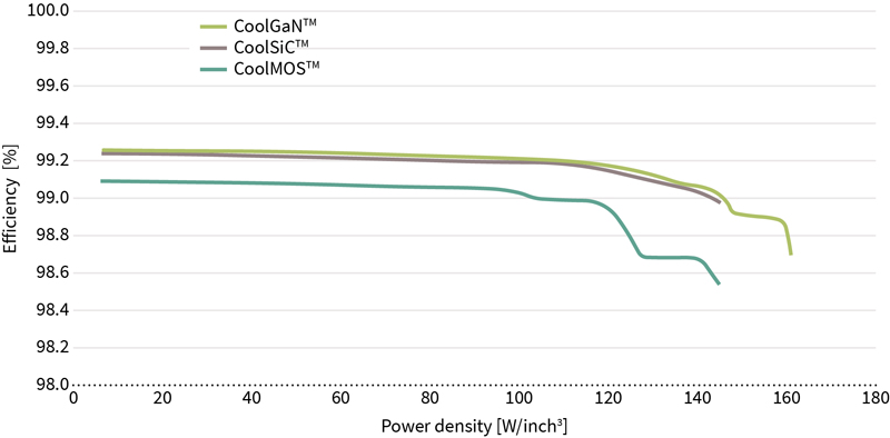
Concerning the combination efficiency vs. power density, the Pareto front analysis result [1, 4, 5] in Figure 6 shows that GaN and SiC are substantially equivalent in the CCM totem-pole PFC. Only GaN can provide power density up to 160 W/in³ but only at efficiency significantly < 99 percent.
Click image to enlarge
Figure 6: Optimization result for the totem-pole PFC stage, including EMI filter, comparing system efficiency versus density for GaN-, SiC-, and Si-based power devices, respectively
We can conclude that thanks to the easier driving scheme than GaN, SiC is the preferred choice of semiconductor for the CCM totem-pole PFC stage of telecom SMPS.
LLC stage
The combination of high efficiency and power density is also crucial for the LLC stage. In resonant topologies, such as LLC, there are more options to increase the switching frequency to minimize the magnetic size, mainly thanks to the ZVS behavior, which intrinsically reduces the power devices switching losses.
The study of the LLC topologies in a rectifier aiming to ≥ 98 percent efficiency at 50 percent load is depicted in [3]. Infineon’s CoolGaN™ e-mode HEMT 600 V technology has been proven to be the only technology able to keep efficiency higher than 99 percent in an interleaved FB LLC topology at a resonant frequency up to 500 kHz. Figure 7 briefly reports this result. Using MV CoolGaN™ [1] technology in the synchronous rectification at the secondary side plays an essential role in this achievement.
Click image to enlarge
Figure 7: CoolGaN™ vs. CoolSiC™ vs. CoolMOS™ efficiency levels at 50 percent load condition
The Pareto efficiency vs. power density optimization methodology applied to the LLC stage confirms this result [4]. For this optimization, the primary side is varied between the different technologies of Si, SiC, and GaN, with the secondary side always using Si devices in the synchronous rectification (SR) stage. Additionally, a fourth optimization is performed with GaN both on the primary and secondary sides, employing the upcoming 100 V CoolGaN™ devices [2] in the SR stage (see Figure 8).
Click image to enlarge
Figure 8: Optimization results for the LLC stage showing efficiency versus power density for Si, SiC, and GaN-based power devices
From Figure 8, it is clear that GaN enables higher efficiency than SiC at the highest power densities, where the switching frequencies are higher. The all-GaN solution achieves an additional gain in efficiency of 0.2...0.3 percent in comparison to the one with GaN only on the primary side. Furthermore, the maximum power density of the all-GaN is around 10 percent higher than the next best GaN with Si SR stage. The main reason for this is the lower input and output capacitances charge of the 100 V CoolGaN™ devices compared to the MV Si counterparts. In turn, this gives benefits in the design of the resonant tank by allowing less circulating current as less current is required to change the secondary side’s polarity.
We can conclude that, concerning the figure-of-merit (FOM) efficiency vs. power density, the best solution for the LLC stage of a telecom rectifier is to use CoolGaN™ technology on both primary (HV) and secondary synchronous rectification stages (MV).
Reliability for telecom rectifiers in 5G era
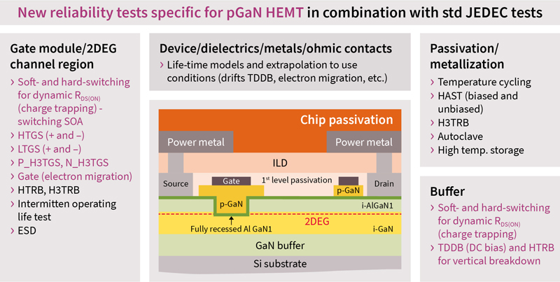
Reliability is the second fundamental requirement for telecom rectifiers in the 5G era. Infineon’s white paper [6] outlines the comprehensive and application-specific qualification process that Infineon has followed to ensure that HV and MV CoolGaN™ technologies meet the target lifetime and quality requirements, including telecom rectifiers mission profile. The substantially different structure of GaN devices compared to Si ones leads to a different qualification plan. Figure 9 briefly shows the new reliability tests specifically implemented by Infineon on the CoolGaN™ technology.
Infineon follows a comprehensive qualification regime for its CoolSiC™ devices to ensure reliable performance in real-world operating conditions and applications, including the telecom environment [7]. Despite the similarities to Si devices, e.g., the vertical device structures, there are still significant differences in the material properties and the operating modes of these new power devices. As these differences are substantial, their impact on the final application’s operation and the reliability qualification processes have been carefully considered.
Driven by its dedication and commitment towards high quality, Infineon was among the companies that have initiated and contributed to establishing GaN and SiC focused subcommittees within JEDEC (respectively JC-70.1 and JC-70.2) to introduce qualification guidelines and standards regarding WBG devices.
Click image to enlarge
Figure 9: New reliability tests specifically implemented by Infineon on the CoolGaN™ technology in combination with standard JEDEC tests
An essential reliability requirement for HV devices in telecom rectifiers is the so-called cosmic ray ruggedness. Semiconductor devices are subject to nuclear particle irradiation during their whole lifetime. The irradiation is governed by the neutron flux, which increases exponentially with altitude. To calculate the cosmic radiation failure rate of HV devices, the mission profile of the specific application, i.e., applied voltage, junction temperature, and altitude vs. respective operating hours, has to be considered. In some installations, telecom rectifiers must operate continuously up to 4000 m (13000 ft) a.s.l.
Both CoolGaN™ and CoolSiC™ devices have been developed and qualified to guarantee the necessary cosmic ray ruggedness. The breakdown voltage of the HV CoolGaN™, being significantly higher than the rated 600 V, represents by itself an important feature from this point of view. The cosmic ray ruggedness of the CoolSiC™ MOSFET 650 V has been tuned, as for any vertical power device, by a proper balance of thickness and doping of the drift or base layer. In this way, it achieves the best trade-off between radiation robustness and on-state losses.
Summary
This article presented an overview of the main requirements in modern telecom SMPS, directly derived from the key trends in 5G Systems.
We demonstrated how Infineon’s MV and HV CoolGaN™ e-mode HEMT and CoolSiC™ MOSFET 650 V technologies effectively address all main requirements in this field by covering both performance and reliability aspects in the latest generation of telecom rectifiers.
To discover more about Infineon’s broad portfolio of wide-bandgap products and solutions designed to meet the requirements of modern telecom rectifier applications, be sure to visit our WBG website.
[1] More details on MV CoolGaN™ products will be available soon
[2] More details on MV CoolGaN™ products will be available soon
References
1: G. Deboy “Design guidelines for high power server and telecom power supplies use-cases,” PSD Magazine, May 2021
2: G. Deboy, O. Haeberlen, and M. Treu, “Perspective of loss mechanisms for silicon and wide bandgap power devices,” CPSS Transactions on Power Electronics and Applications, vol. 2, no. 2, pp. 89–100, 2017.
3: F. Di Domenico “All Semiconductor Switch Technologies Lead to Rome”, PSD Cover Story, March 2020
4: Matthias Kasper and Sam Abdel-Rahman, “How to reap the benefits of wide-bandgap semiconductors in server applications”, PSD magazine, May 2021.
5: J. W. Kolar, J. Biela, and J. Miniboeck, “Exploring the Pareto Front of Multi-Objective Single-Phase PFC Rectifier Design Optimization - 99.2 percent Efficiency vs. 7kW/dm3 Power Density,” in Proc. of the 6th Int. IEEE Power Electronics and Motion Control Conference (IPEMC), pp. 1–21, 2009.
6: T. McDonald “Reliability and qualification of CoolGaN™”, Infineon Technologies White Paper 10-2018
7: “How Infineon controls and assures the reliability of SiC based power semiconductors”, Infineon Technologies White Paper, 07-2020


