Server / Telecom - Si and WBG solutions: Part 4 of 4 Editorial Series Sponsored by Infineon; Design Guidelines for High Power Server and Telecom Power Supplies Use-Cases
Technology perspective and value-added features of wide bandgap power semiconductor devices
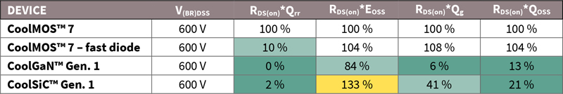
Table 1a: Key performance indicators of silicon (Si)-based superjunction technology CoolMOS™ C7 compared to SiC MOSFET CoolSiC™ and GaN HEMT technology CoolGaN™
Introduction
With the recent introduction of active wide bandgap (WBG) power semiconductors on a broad commercial scale, the number of use cases is rapidly increasing. High power applications such as power supplies for server and telecom have been among the first adaptors driving acceptance and early success stories.
For server power supplies, the rapidly increasing power demand of modern artificial intelligence (AI)-assisted processors drives power requirements per server continuously up, reaching now more than 2.5 kW. As the form factor of power supplies being mounted directly onto the motherboard remains the same, power density has massively increased to 85 W/in³ and beyond. Similarly, power for remote base stations is rapidly increasing in the wake of the roll-out of the 5G infrastructure. To avoid costly cabinets on the floor, equipment such as the AC-DC power supplies must move up on the pole, closer to the antennas. In these applications, ultra-flat designs (1/2 U height) and passive cooling pose stringent requirements for the power supply’s density and efficiency. Finally, hyper-scale data centers, with their continuous striving to optimize total cost of ownership, have pushed efficiency both for 48 V and 12 V eco-systems to hitherto unreached limits.
This article aims to provide guidelines regarding the value and best use cases for GaN- and SiC-based power semiconductor devices compared to their silicon counterparts. The analysis derives key performance indicators from a device-physics-based view and discusses their potential for further improvement from a technology perspective [1].
We follow the typical design considerations in a switch-mode power supply (SMPS), starting with device selection for the power factor correction stage, the primary side isolating DC-DC converter, and, finally, for the synchronous rectification on the secondary side.
Key performance indicators for wide-bandgap semiconductor devices
We use for the comparison of devices rated at 600 V blocking capability four key performance indicators, namely RDS(on)*Qrr, RDS(on)*EOSS, RDS(on)*Qg, and RDS(on)*QOSS as outlined in Table 1a.
The following figures-of-merits (FOM) can be linked directly to switching transitions in SMPSs:
· RDS(on)*EOSS is a measure for the switching losses in hard switching single-ended circuits,
· RDS(on)*QOSS is an indicator for the amount of current needed for soft switching transitions, and
· the sum of Qrr and QOSS represents the switching losses in a half-bridge circuit in case of hard commutation [2].
GaN HEMT devices (such as Infineon’s CoolGaN™ technology), with their absence of a blocking pn-junction, have zero reverse recovery charge, which is a unique advantage in applications such as motor drive PV inverter, and totem-pole PFC stages. Depending on the modulation scheme, hard commutation of the load current may occur in every switching cycle in these applications. Also, SiC MOSFETs (such as Infineon’s CoolSiC™ technology) are excellent concerning commutation losses in a half-bridge circuit. Here, the extremely short ambipolar lifetime of electrons and holes reduces the electrically visible Qrr contribution on the device’s terminals. In silicon devices, ambipolar lifetime adjustments, employing Pt-diffusion or ion-irradiation, are limited by the increase of drain-to-source leakage currents. However, this is not the case for wide bandgap devices, which can offer a much broader optimization range.
Click image to enlarge
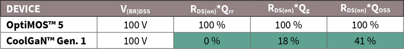
Table 1b: Key performance indicators of Silicon-based shielded-gate technology OptiMOS™ 5 compared to GaN HEMT technology CoolGaN™
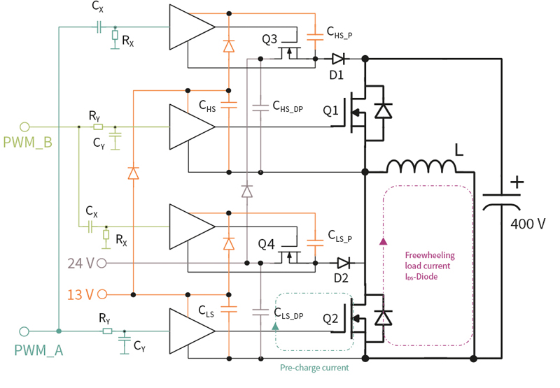
The large reverse recovery charge of superjunction (SJ) devices does not allow continuous hard commutation of the body diode even in fast diode versions with reduced ambipolar lifetime. Nevertheless, from an application perspective, two solutions exist.
First, the so-called triangular current modulation scheme (TCM), where the load current reverses its direction. In this case, the load current discharges the switching node capacitance allowing both ZVS operation of the switch to be turned on as well as complete removal of the Qrr charge of the switch previously conducting on its body diode. The regulation requires variable switching frequency with load and input voltage and precise detection of the zero-current crossing.
A second approach is the injection of a current pulse into the switching node, momentarily overriding the load current and pre-charging the device, which previously conducted on its body diode, to a low voltage of, e.g., 20 V [3]. This solution allows fixed-frequency operation with continuous-current modulation (CCM) through adding few components for the auxiliary current injection circuit.
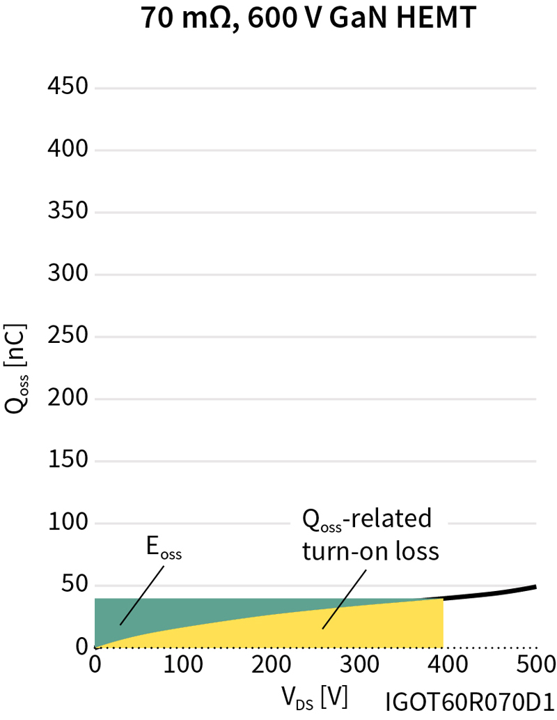
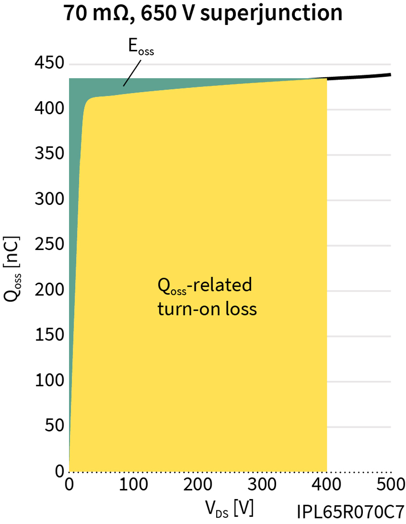
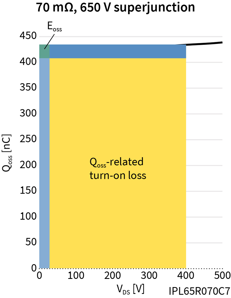
It is noteworthy to take a closer look at this concept from a technology perspective. Figure 1 shows a representation of QOSS as a function of the voltage for the Gen1 GaN HEMT (Fig. 1a), the latest SJ technology CoolMOS™ C7 (Fig. 1b), and a graphic visualization of the loss saving potential for SJ devices with the current injection method (Fig. 1c).
Click image to enlarge
Click image to enlarge
Click image to enlarge
Figure 1a, 1b & 1c: Comparison of QOSS as a function of voltage for Gen1 CoolGaN™ (Figure 1a), CoolMOS™ C7 (Figures 1b & 1c). The blue shaded areas represent the resulting losses when a novel current injection method is used
The areas colored in yellow represent the QOSS-related losses at turn-on. This is the contribution of charge flowing from the device previously conducting into the device turning-on while operating in linear mode at DC link voltage level. The green area is the amount of energy stored in the output capacitance of the device previously blocking. This energy will be dissipated as Joule loss inside the device by opening the channel and have the electron current discharge the output capacitance. In a hard commutation event with the high side device conducting on its body diode, the yellow-colored area represents the losses associated with the high side device, and the green area represents the losses associated with the low side device turning on. The sum of both areas indicates the total losses.
The GaN technology is a prime candidate for hard commutation with its factor 10 lower QOSS charge and its very balanced loss contributions from EOSS and QOSS, respectively. Specifically, in the light of the large QOSS contribution, SJ devices seem not to be able to compete. However, this is exactly where the current injection scheme overcomes hitherto-seen limitations: pre-charging the switching node from a low voltage source removes both Qrr and a large portion of the QOSS contribution. As this charge is extracted to a low voltage supply, the light blue area represents the associated losses. Consequently, the remaining QOSS contribution creates only a fraction of the original losses; this loss is shaded respectively in blue in Figure 1c.
From a technology perspective, the extreme non-linearity of the output capacitance of SJ devices leads in combination with the current injection method to an optimization path with continuously decreasing pre-charging losses and at the same time ever lower commutation losses in the half-bridge circuit.
From a loss balance view, the current injection allows SJ devices to be on par with GaN in single-ended applications and half-bridge-based circuits. With the progress to smaller cell pitches, SJ devices benefit both from a lowering of the depletion voltage of its inner pn-column structure – making the light blue shaded area more narrow – and from a reduction of the remaining QOSS contribution between the depletion voltage and the DC link voltage – making the blue shaded area flatter. In comparison, the GaN HEMT technology can benefit from reducing its active area, which likewise improves the QOSS contribution being derived from the drain-to-substrate portion of the output capacitance.
In the class of 100 V-rated devices, Qrr and QOSS contributions are typically in the same order of magnitude for modern shielded-gate power transistors. The GaN technology clearly shows significant advantages in both parameters lowering half-bridge commutation losses to less than one-fifth of its silicon counterpart. Also, the gate charge is by more than factor 5 lower, which are perfect pre-requisites for high-frequency operation. Table 1b shows the comparison.
Technology positioning for high power applications
PFC stage
Compared to their silicon counterparts, the attractiveness of wide-bandgap technologies depends mainly on the application’s requirements concerning efficiency and density. For power factor correction stages below 98.5 percent efficiency or power supply efficiencies below titanium level, the solution dominating the market is AC rectification with a diode bridge followed by a boost circuit.
In this segment, the combination of SJ technology with a SiC Schottky barrier diode will prevail in the market. Both the rich portfolio of devices allowing near unlimited fine-tuning of conduction losses and the consequent optimization of the switching losses make CoolMOS™ the prime choice. The switching transition from a conducting SiC diode to the Superjunction device at hard turn-on creates losses from the diode being proportional to Qc*VDC with Qc being the capacitive displacement charge of the SiC diode and losses in the switch turning on, which are proportional to EOSS. The extreme optimization of the EOSS contribution in SJ devices has brought this parameter now on par with GaN and even below SiC power devices. With upcoming progress in the cell pitch in the CoolMOS™ C8 family, EOSS can be further reduced. The non-linearity of the output capacitance helps at the turn-off to shut down the channel current effectively before the voltage across the switch rises, thus enabling a loss-less turn-off.
For power supplies at titanium level efficiency and beyond or stringent power density requirements as, e.g., in telecom base stations [4], (semi-) bridgeless PFC solutions take continuously higher market share. Here, we see the totem-pole configuration with CCM or TCM control using wide-bandgap or silicon power devices, respectively, in its high-frequency leg and very low-ohmic SJ devices in its low-frequency leg.
The key argument for wide bandgap power devices is the simplicity of control using typically fixed frequency trapezoidal current modulation schemes. Both GaN HEMTs and SiC MOSFETs are used in recently released designs. Specifically, SiC MOSFETs have an advantage as their very low-temperature dependence of the RDS(on) allows using relatively high-ohmic and, hence, cheaper power devices [5].
SJ devices may be used in totem-pole circuits either by applying TCM control with variable frequency or by using the current injection scheme discussed in the previous chapter [3]. All solutions surpass 99 percent efficiency in the PFC stage.
DC-DC stage
Again, efficiency and power density requirements guide the designer towards choosing the best fitting device technology.
For primarily efficiency-driven applications such as power supplies for hyper-scale datacenter, ultra-low ohmic SJ devices combined with precise dead-time control and a careful resonant tank design of the LLC converter are the first choice. With resonant switching frequencies around 100 kHz, the inevitable (relatively long) dead times of modern SJ devices are not yet limiting and do not lead to a substantial increase of RMS currents.
When the power density approaches 70 W/in³ or more, and the LLC converter’s resonant frequency is designed to 300 kHz and beyond, both SiC MOSFETs and, specifically, GaN HEMTs create clear value. The key argument in favor of wide-bandgap devices is their lower RDS(on)*QOSS FOM enabling shorter dead times. Also, control schemes such as 3-level modulation, which effectively limit the LLC’s frequency range, induce hard commutation transitions, especially during a light load operation. In this case, a very low or even zero reverse recovery charge is an advantage. At very high switching frequencies such as 600 kHz and higher planar magnetics become a favorable design option as they create even lower losses than conventionally wound transformers. In this design space, GaN technology is clearly the preferred choice due to its better dynamic figure-of-merits and significantly lower gate charge
The choice of devices for synchronous rectification depends mainly on the switching frequency. During the secondary side switching transition from a (synchronously) conducting state to blocking, the Qrr charge creates additional losses, whereas the charging and discharging of the output capacitance is basically loss-less as long as lumped resistances in series with the output capacitance are negligible.
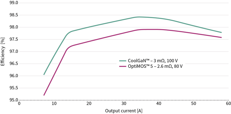
Hence, the use of, e.g., 100 V-rated GaN HEMTs with their zero reverse recovery charge creates a significant benefit when being used as synchronous rectification switch. Figure 2 shows the comparison of OptiMOS™ 5 to CoolGaN™ in an LLC converter delivering 3.6 kW at 52 V output. The design uses two secondary-side paralleled stages in full-bridge configuration, with two devices being paralleled in each position. The converter runs at 270 kHz with 97.9 peak efficiency using silicon devices and at 340 kHz at 98.5 percent peak efficiency with GaN HEMTs.
Click image to enlarge
Figure 2: Efficiency comparison of 100 V-rated CoolGaN™ versus 80V-OptiMOS™ 5 devices used as synchronous rectification switch in a 3.6 kW LLC converter
In a nutshell
High power applications such as power supplies for server or telecom may use a wide range of topologies, modulation schemes, and power devices.
Depending on efficiency and density requirements, several combinations will prevail in the market. Below titanium-level efficiency, the “all-silicon” designs using SJ devices both in “classic” boost type PFC and LLC stages with silicon-based synchronous rectification devices on the secondary side will dominate the market.
For efficiency-driven applications at moderate power density requirements of around 40 W/in³, hybrid combinations using wide bandgap power devices in a bridgeless PFC configuration and a subsequent “all-silicon” LLC converter will gain share. SJ devices in bridgeless PFC circuits are enabled both by triangular current modulation and through a relatively simple current injection circuit.
Finally, in high-density applications at or beyond 70 W/in³ “all-GaN” designs or hybrid combinations with SiC in the PFC stage and GaN in the LLC stage will win. Figure 3 shows Pareto front optimization [6] for a 7 kW power supply unit delivering 54 V. Clearly, the “all-GaN” design wins both in power density and efficiency.
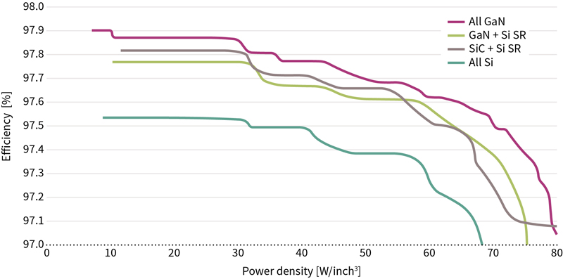
Click image to enlarge
Figure 3: Pareto front optimization of a 7 kW power supply delivering 54V
With its complete technology portfolio strategy offering both SiC MOSFETs, GaN HEMTs, and leading-edge silicon power devices, Infineon Technologies is ready to support high-power applications always with the best fitting selection of power devices. Drivers and control ICs complement the portfolio. For more details, please find the complete offering online.
References
1: G. Deboy, O. Haeberlen, and M. Treu, “Perspective of loss mechanisms for silicon and wide bandgap power devices,” CPSS Transactions on Power Electronics and Applications, vol. 2, no. 2, pp. 89–100, 2017.
2: mM. Kasper, R. Burkart, G. Deboy and J. W. Kolar, “ZVS of Power MOSFETs revisited”, IEEE Transactions on Power Electronics, Vol. 31, No. 12, pp. 8063-8067, December 2016.
3: Rafael Garcia, “Innovative silicon solution for highest PFC efficiency,” PSD magazine, May 2021.
4: Francesco di Domenico, “Towards efficient, reliable, and cost-effective power supply units for 5G telecom rectifier applications using wide-bandgap semiconductors,” PSD magazine, May 2021.
5: Matthias Kasper, Sam Abdel-Rahman, and Juan Sanchez, “How to reap the benefits of wide-bandgap semiconductors in server applications,” PSD magazine, May 2021.
6: J. W. Kolar, J. Biela, and J. Miniboeck, “Exploring the Pareto Front of Multi-Objective Single-Phase PFC Rectifier Design Optimization - 99.2% Efficiency vs. 7kW/dm3 Power Density,” in Proc. of the 6th Int. IEEE Power Electronics and Motion Control Conference (IPEMC), pp. 1–21, 2009.