Shrinking Industrial Designs with Highly Integrated PMICs
ICs that integrate several functions in the same package, along with optimized passive components, can help shrink the overall PCB space required.
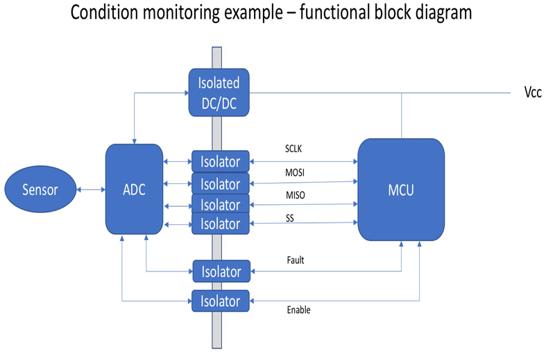
Figure 1: Functional block diagram of a condition monitoring analog front end attached to a host microcontroller (Source: Mouser)
The industrial manufacturing landscape is undergoing considerable change. Led by government initiatives such as Industry 4.0 and the associated Industrial Internet of Things (IIoT) trend, organizations are keen to embrace and harness the data gathered from a vast army of connected sensors. Promising to yield analytical insight that can make manufacturing operations more operationally efficient, these schemes have many potential benefits. A connected factory enables implementation of a predictive maintenance-based maintain, repair and operate (MRO) regime, for which condition monitoring of wearing parts, for example by detecting a motor’s bearing wear through a vibration sensor, is essential. These new insights, and the ability to optimize operations can unleash the capability of an organization to entirely transform its facilities into a service-based operation. In fact, many industrial manufacturing equipment suppliers are doing just that.
However, making an industrial data-led environment requires substantial amounts of equipment, from compact sensors and robust communication gateways to essential programmable controller hardware. Not only is there a significant cost associated with this equipment, but there is also the consideration of where it might be placed on the factory floor. Plant floor space is at a premium, so all the control equipment for a specific manufacturing line typically needs to be located within a single control cabinet. In turn, this means more and more electronics-based systems need to be squeezed into a constrained space. To create smaller designs, engineers are tasked with selecting the smallest possible passive components and ICs. In addition to small size, these components must have optimized thermal management and low EMI properties to allow higher levels of integration so solutions are more compact – and to avoid heat management challenges, they must also be more energy efficient.
Application Example
In addition to making designs smaller, engineers must contend with developing products that can function reliably in an electrically noisy environment. Increased automation results in a concentration of electrically driven machinery, for example using motors and actuators that can create high voltage transients. Transient spikes are damaging to sensitive circuitry and can interfere with reading accurate sensor measurements, and this is particularly the case where analog signals are involved. The trend is to convert analog signals into the digital domain as soon as possible after measurement, but this still leaves analog-to-digital converter (ADC) and digital-to-analog converter (DAC) circuitry prone to such conducted transients. Isolation, the electrical or galvanic separation of a signal, is a technique that mitigates the effects of transients. Isolation is also required to avoid damage to the attached circuitry, as well as for the purposes of electrical safety certification. Isolation between a sensor and its associated ADC and a host microcontroller, is a prudent step. In a condition monitoring example, the sensor is directly attached to a motor that is probably line-powered, presenting a potential path for stray voltages back to the host. Isolation ensures that damaging voltage spikes or leakage currents present at the sensor or ADC never reach the microcontroller. In this example, the ADC would also need to be powered by an isolated supply. To achieve this degree of isolation requires both power and data signal isolation and would typically be architected using an isolated DC-DC converter and digital signal isolation ICs – see Figure 1.
Reducing the BOM and PCB Footprint
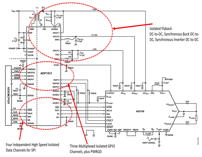
By integrating the power conversion and management, power isolation and digital signal isolation (SPI) within a single IC saves considerable board space in addition to the potential for bill of materials reductions. An example of an IC that integrates all of these functions within a single LFCSP 7mm x 9mm compact package is the ADP1031 from Analog Devices. Capable of operating across a wide supply voltage range, from 4.5V to 60V, the ADP1031 hosts three micropower DC-DC converters including an isolated flyback regulator, an inverting regulator and a buck converter within its micropower management unit (PMU). Total power delivery capability is up to 2.0W with an energy efficiency between 80% and 90%. Four bidirectional high-speed isolation channels, accommodating an SPI interface, and three isolated general-purpose I/O channels that use Analog Devices’ patented iCoupler technology, complete the architecture of the IC – see Figure 2.

Click image to enlarge
Figure 2: Key features of the Analog Devices ADP1031 three-channel, isolated micropower management unit with seven digital isolators illustrated with external components including the flyback converter transformer (Source: Analog Devices)
The power management unit includes a soft-start power-up capability, input over-current, and output over-voltage protection features in addition to a number of programmable flyback and inverter converter options. The ADP1031 includes an internal MOSFET switch for the flyback converter and requires only a minimum of external passive components and the flyback isolation 1:1 ratio transformer to operate. Input to output isolation across all three power domains is 300V. Also, the ADP1031 permits control of the converter slew rate to facilitate improving EMI performance in addition to conforming to CISPR11 (EN 55011) Class B radiated emission levels.
The ADP1031 is optimized for use with the Analog Devices AD5758, a single-channel 16-bit resolution DAC IC – see Figure 3. Used together, the ADP1031 and the AD5758 speed the design process by offering certification against basic 300V isolation requirements, and this is a low-risk route for engineers to take.
Click image to enlarge
Figure 3: Analog output application powering an Analog Devices AD5758 DAC (Source: Analog Devices)
Transformer and Inductor Selection
When optimizing the design of the flyback converter for ADP1031, the choice of transformer must be considered. The ADP1031 feedback scheme eliminates the need for a feedback winding in the flyback transformer, which thus consists of a single primary and single secondary winding. This simplification leads to smaller transformers with lower DCR and lower leakage inductance and especially makes the design engineer’s task easier by making it possible to select an off-the-shelf transformer. Selecting a well-designed, miniature transformer with low leakage inductance and d.c. resistance can have a significant impact on the design’s EMI characteristics and energy efficiency. The needed transformer ratio will be determined by the choice of input and output voltages. In collaboration with Analog Devices, transformer specialist Coilcraft has developed two transformers specifically for use with the ADP1031 part. These are the Coilcraft WA8478 and the Coilcraft YA9293, and both are 1:1 ratio, accommodate a 4.5V to 60V input voltage, a 2250Vrms isolation and designed with creepage and clearance for Basic insulation. . The transformers also have AEC-Q200 Grade 1 qualification, making them suitable for use in automotive applications where the ambient temperature range is from -40°C to +125°C. Nominal leakage inductance is 1.2µH for the WA8478 and 1.62µH for the YA9293 part.
Coilcraft also offers PA6594-AE 47 µH inductor that is optimized for use with the integrated buck converter feature of Analog Devices AD5758 16-bit DAC IC. The PA6594-AE inductor has a compact footprint and is only 1.8 mm in height.
Conclusion
With today’s space-constrained designs, selecting ICs that integrate more than one function within the same package, along with optimized passive components can assist in shrinking the overall PCB space required. The ADP1031 meets this requirement by combining power management and serial communication isolation in a 7mm x 9mm package. Using the ADP1031 along with optimized Coilcraft transformers provides high performance and small solution size.