In space exploration, social isolation is often the norm. Likewise, isolation has always been part of how MOSFET semiconductors operate….
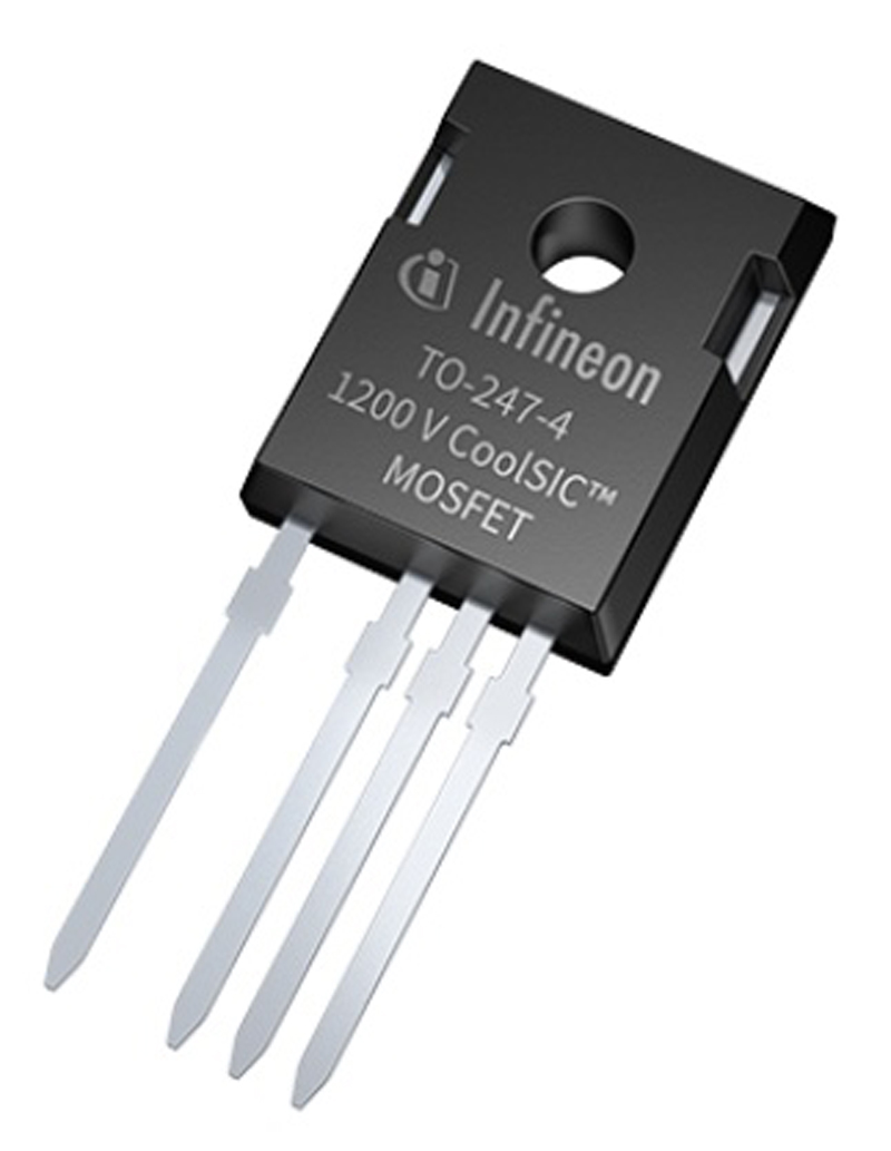
Figure 1: Infineon Technologies CoolSiC 1200V SiC Trench MOSFETs support higher switching frequencies with reduced heat dissipation in a space-saving package. (Source: Mouser Electronics)
Business magnate, industrial designer, and engineer Elon Musk is aiming to land humans on Mars by 2026. Musk’s vision is leading humanity to explore more of space. In contrast, power systems designers are primarily concerned with saving space on their physical layouts of power systems designs. Not to be confused with the race to find more inhabitable space on distant planets, we’ll examine wide bandgap material components and integrated architectures, two techniques that designers should consider when they desire to save space. Let the race for smaller, integrated power systems design begin.
MOSFETs: A Critical Power Switching Component
MOSFETs are voltage-controlled devices. In a MOSFET, the Gate (G) electrode is electrically isolated from the Drain (D) and Source (S) terminals. The electrically isolated high impedance path is created by a thin layer of insulating material placed in the semiconductor in the form of metal-oxide, resulting in MOSFETs having a very high input impedance. Suppose a MOSFETs high input impedance receives a threshold voltage to the Gate. In that case, a low impedance path is made for signals and power to flow between previously isolated circuits. MOSFETs find ubiquitous deployment as power switches because of these unique characteristics.
Wide Bandgap (WBG) Semiconductors
Designers can seize the opportunity for size reduction with the employment of wide bandgap (WBG) semiconductor materials. Compared to Si-based components, WBG devices allow for smaller device sizes with higher switching frequencies, lower mass, and lower losses providing increased power efficiencies. WBG semiconductors’ additional advantages over Si in power electronics include higher operating temperatures, robustness in harsh environments, and high breakdown voltages. WBGs save space in a wide variety of applications, including industrial functions, such as motor drives and power supplies, and automotive and transportation systems, including hybrid and electric vehicles (HEV/EV), PV inverters, railway, and wind turbines. Suppliers producing these products include an assortment such as Infineon Technologies, Wolfspeed/Cree, Qorvo, ON Semiconductor, STMicroelectronics, ROHM Semiconductor, and GaN Systems.
Silicon Carbide (SiC)
Silicon carbide (SiC) offers a wide bandgap of three electron volts (eV) and a much higher thermal conductivity compared to silicon (Si). Perfectly suited for high breakdown, high-power applications that operate at high-frequency SiC-based MOSFETs can be employed advantageously into 1200V target photovoltaic inverters, battery charging, and energy storage applications. Infineon Technologies’ ultra-fast switching family of CoolSiC™ is an excellent example (Figure 1).
SiC-based MOSFETs device parameters, such as the RDS(on), change less with temperature than traditional silicon (Si). The thermal conductivity of SiC is close to 10 times (10x) greater than that of silicon (Si) (Figure 2). Higher thermal conductivity makes it easier for a semiconductor to dissipate any heat generated. Because heat can be distributed more effectively with SiC, it can often eliminate the need for fans and heat sinks, facilitating smaller-sized designs for power applications. These factors enable designers to work within tighter margins in their plans, allowing them to deliver extra performance.

Click image to enlarge
Figure 2: Design engineers face an ongoing mission to reduce component size
SiC MOSFETs can be employed with complementary parts that take further advantage of WBG materials. SiC MOSFET Gate Drivers are appropriate products to drive SiC MOSFETs. Gate drivers help control the power and switching characteristics of the power MOSFET. Engineers work to ensure that the impact of electromagnetic interference (EMI) and voltage ringing does not interfere with the specification requirements necessary to ensure reliable performance. Gate drivers generally provide a wide range of typical output current options. SiC gate drivers might incorporate critical features and parameters for driving SiC MOSFETs. These features include tight propagation delay matching, precise input filters, wide output-side supply range, negative gate voltage capability, active Miller clamp, desaturation detection circuit function (DESAT) protection, and extended common-mode transient immunity (CMTI) capability.
DC-DC Converters
Like power MOSFETs, DC-DC converters proliferate any power system design. DC-DC converters are fundamental building blocks used in electronics power-management circuits. They convert one direct current (DC) voltage to another DC that is either a greater (step-up, boost) or lower (step-down, buck) voltage. Making small-sized DC-DC converters is a goal of many electronics component suppliers.
DC-DC Buck Regulators
Newly introduced DC-DC buck regulators have an almost 2x reduction in footprint and a one-third decrease in height with significant improvements in power efficiency, transient performance, and EMI compared to previous versions. This improvement is facilitated by developing new part architectures that yields a smaller size and higher efficiency DC-DC converter design.
Buck regulators often utilize internal power MOSFETs. In the drive to reduce the size and simplify buck regulators, especially for low output currents (< 20A), many parts are offered with a controller and integrated FETs within one package. A controller with an integrated FET can compromise efficiency because, in specifying for a wide range of applications, these FETs’ voltage ratings can be much higher than those needed for a given application, resulting in increased switching losses. Also, the dimensioning of the MOSFETs will almost certainly be sub-optimal for a specific duty cycle. This latter point can be a significant compromise, especially for low-duty cycle applications.
Packaging technology is deployed to reduce the size and squeeze every possible milliohm of parasitic losses from the powertrain to glean efficiency improvements. Integration of complete powertrains—control-plus FETs, output inductor, and input/output filters—is impeded primarily by the physically large inductors that are still required.
Novel Approach
A novel approach resolves many of the traditional Buck regulator design issues. It allows switching frequencies to remain in the 1MHz to 2MHz range while reducing the amount of inductance required, plus improving overall power conversion efficiency. The breakthrough employs a two-stage architecture comprising a charge pump, a switched-capacitor converter, with a switched-mode power supply. Their specific charge pump design solves fundamental issues traditionally associated with charge pumps, namely low efficiency, and high EMI. The current source employed is, in effect, an inductor in a buck stage. This inductor is a close approximation to a current source and is used to absorb all of the charge redistribution losses typically made in the switch. Because this current source inductor can be in the output stage, the energy, rather than being lost, can be recycled as useful energy to the load. This recycled energy allows the series resistance of the charge pump switch (and associated parasitic impedances) to be made as small as possible because in-rush current is no longer an issue and minimizes the charge redistribution losses in this part of the circuit. The charge pump can realize power efficiencies of 97 percent to 99 percent.
The charge pump itself is also two-phased, interleaved, and presents to the input almost 100 percent duty cycle. Compared with a traditional buck regulator, where the duty cycle might be only 10 percent, this makes a massive difference to the input current ripple and the amount of input filtering needed. In tests, the supplier has measured at least 5x lower input current ripple than an equivalent single-stage buck.
This two-stage buck is an architectural innovation using standard off-the-shelf FETs in a very mature complementary metal-oxide-semiconductor (CMOS) semiconductor process. Because the inductor is no longer the dominant component in the bill of materials (BOM), power conversion shrinks from occupying typically 30 percent to 40 percent of a system’s circuit area to half of that, without compromising efficiency. Furthermore, because the inductor usually is one of the tallest components in a system, this architecture allows for thinner solutions, improving packing density, and enabling mobile products to be slimmer.
Conclusion
Together, we have looked at how wide bandgap material components and integrated architectures might be two techniques that power supply designers might consider when they desire to save physical board space in their next design. Your mission is to race ahead and design innovative power systems solutions that use fewer components and occupy less board space.