SiC MOSFET Efficiency and Protection without Compromise
The efficiency and size benefits of SiC devices have been embraced by designers of industrial, automotive, traction systems and photovoltaic power conversion
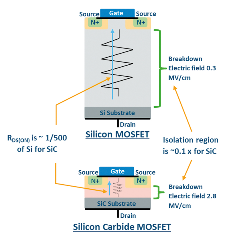
Figure 1. Comparing SiC with conventional Silicon MOSFETs reveals the clearly superior semiconductor characteristics of the SiC material, which allows the construction of significantly smaller switching devices
The lower sheet resistance of wide-bandgap SiC materials (typically 1/100th that of conventional silicon) results in smaller devices for a given current capacity – valuable in space saving applications. In addition, the electric-breakdown- field for SiC (approximately 2.8 MV/cm) allows for a much shorter isolation region within the material. A significant benefit is that the smaller size of SiC switches reduces parasitic capacitance, which improves switching efficiency and allows the switch to operate at higher frequency without penalty. These are clear benefits however, the reduction in the mass of the switch means that protection circuitry has to operate very quickly in order to prevent thermal damage. Shutdown in less than 3 µs is a common requirement for SiC devices (as compared to the 10 µs seen with conventional IGBT and MOSFET switches).
SiC technology is relatively new in the mainstream, and there are different device structures being used as the MOSFET designers work the new material. Cascode and MOSFET configurations with different gate characteristics have resulted in a wide range of gate voltage requirements, further challenging the circuit designer. As with all switches, protection circuitry is required to safely turn off the switch in the event of a system short-circuit. Desaturation detection must avoid false tripping and this typically results in a switch blanking time of up to 2 µs – a significant portion of the thermally limited high current time envelope. Fast turn off (rapid di/dt) may induce VDS overvoltage during shutdown so shutdown rate must also be controlled.
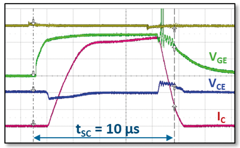
Figure 2 shows a typical gate drive circuit for an IGBT switch and associated short circuit shutdown characteristic. During a short circuit shutdown, VCE rises above the DC Link voltage and causes the TVS network to break over delivering current Iac to the gate node. Iac2 charges Cres and causes the gate voltage to rise and turn the switch back on to limit VCE. However switch T2 pulls current Iac1thru gate resistor Rg(off). Increasing Iac3 (via ACL pin) increases the impedance of T2 and reduces Iac1 , but this takes time. The solution is to increase the gate resistance, which will reduce the current drain from the gate node and improve the clamping voltage. Driving and IGBT in this way is effective and the change in gate resistance does not significantly change switch efficiency. However, increasing gate resistance for a MOSFET will reduce switch transition speed, increase switching losses and reduce efficiency.
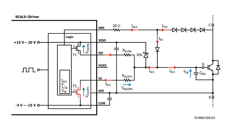
Click image to enlarge
Figures 2a & 2b. IGBT Desaturation Detection and Advanced Soft Shutdown in Operation. IC increases and induces a shutdown (VGE reducing). Subsequent overvoltage (VCE) detection causes an increase in VGE to limit voltage overshoot and complete a safe shutdown of the switch by limiting di/dt
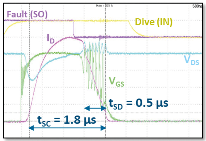
To safely and quickly shut down an SiC Switch without increasing gate resistance requires a different detection and shutdown strategy. Figure 3 Shows an SiC Switch short circuit shutdown using a new control algorithm to provide rapid and controlled switch shutdown.
As before the desaturation triggered shutdown induces a VDS overvoltage to occur, this causes the TVS stack to break over. Iac2 charges Cres. As before, Iac1 begins to flow thru Rg(off) reducing Iac2. However, in this configuration Iac3 induces a rapid response from the IC control logic. In this case the control circuitry rapidly toggles T4 and T5 to alternately sinks and sources Iac1 current. This strong drive reduces effect of Rg(off) on Iac2 making an adjustment in gate resistance unnecessary. This allows fast turn-off and control of VDS without compromising efficiency.
Click image to enlarge
Figure 3. SiC advanced Active Clamping: Toggling current to the gate via T4 and T5 provides a very rapid shutdown while providing an aggresive control of VGS to limit the VDS excursion. Following a 1.3 µs blanking time a desturation-fault shutdown asserts allowing the SiC MOSFET to be turned off in less than 1.8 µs. The toggling of the VGS gate drive can be clearly seen
By removing the role that the gate resistors play in limiting voltage overshoot, the SiC advanced Active Clamping employed in the SiC SCALE-iDriver™ IC family from Power integrations allows the designer to optimize the gate drive resistors to maximize efficiency without compromising performance to insure safe shutdown protection.
How is the gate driving challenge being addressed?
Figure 4 shows typical gate voltage regions for different SiC switch structures. Some devices require a regulated turn-on voltage while others need a regulated negative turn-off voltage to ensure that they do not exceed the gate-source safe operating area as given in their respective data sheets. Typically, only one voltage can be regulated, while the other voltage is dependent on actual load conditions.

Click image to enlarge
Figure 4. Turn on and Turn off requirements for different SiC switch types. The requirements are often mutually exclusive – making the design of the ‘universal SiC gate driver’ more challenging
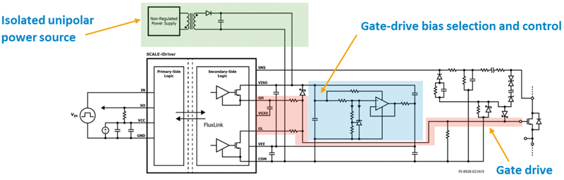
To create a stable gate-driver control voltage, various controllers use bi-polar or unipolar supply voltages to provide an isolated driver voltage. A unipolar-based gate driver is shown in figure 5. The power supply delivers a raw supply voltage to the VISO pin of the control IC. In order to match the requirements of a particular SiC MOSFET, an external programming input is required. A gate driver bias circuit is used to adjust the centre point of the drive rails (delivered via the GH and GL pins). A potential divider between VISO and COM pins is used together with a shunt-regulator to control the drive voltage partitioning via the VEE pin. The shunt regulator provides a more temperature and load stable voltage than would a simple Zener diode based solution.

Click image to enlarge
Figures 5a & 5b. A SCALE-iDriver power transformer provides 15 V to the VISO pin and the control IC uses an internal regulator to generate a stable drive voltage, as directed by the bias input. Additional circuit modifications may be required to reduce potential circuit oscillations during turn-on which will be switch dependent
Driving silicon carbide MOSFETs provides significant challenges for the gate-driver circuitry. Traditional control techniques are often inadequate – unable to support the rapid switching and corresponding overvoltage control issues that follow a desaturation (short circuit) event. In addition, the nascent nature of SiC switch design means that there is wide variation in gate-drive voltage requirements. Solutions exist that can provide the rapid control and meet programmability without compromising efficiency or safety in switching circuits.