Author:
Peter Dallimore, DesignSpark, powered by RS Components
Date
03/02/2020
 PDF
PDF

Click image to enlarge
Figure 1. A large driver source current is needed to charge gate capacitances quickly. Source: ON Semiconductor TND6237/D
Silicon carbide power MOSFETs are moving closer to approximate price parity with conventional silicon MOSFETs or IGBTs. Their key advantages are lower RDS(ON) and reduced switching losses, breakdown voltages comparable to IGBTs, and greater temperature capability. These give designers of power-conversion systems such as switched-mode power supplies or inverters more freedom to increase energy efficiency, specify smaller components, and simplify thermal management to minimize size and engineering costs without sacrificing reliability.
Paying careful attention to the design of the gate driver, to ensure optimal performance in the ON state and during switching transitions, is important to maximize these inherent advantages of SiC MOSFETs.
Secrets of SiC Success Bring Switching Challenges
The high breakdown voltage of SiC MOSFETs is the result of the wider bandgap of SiC compared to conventional silicon. Because the electrons require about three times higher energy to move from the valence band to the conduction band, this ultimately allows a SiC MOSFET to withstand about 10 times the breakdown field strength of a comparable silicon device. Regarded from the opposite perspective, the channel thickness can be greatly reduced for a given voltage rating, which results in a lower minimum RDS(ON).
However, SiC MOSFETs behave differently in saturation compared with silicon devices. There is no clearly defined transition between the linear and saturated regions: whereas a silicon MOSFET is more or less turned fully on when VGS exceeds the threshold voltage - causing the device to behave like a non-ideal current source - the SiC MOSFET has generally lower transconductance (gm) and instead behaves more like a variable resistance. The result is that RDS(ON) continues to reduce as the gate voltage is increased towards the maximum allowable limit, VGSmax. Hence, a higher turn-on gate voltage is required to fully realize the superior RDS(ON) of the SiC MOSFET. Because VGSmax can be about 18-25V, depending on the device, the driver must be capable of applying VGS in the range of 15V to 20/22V.
As far as the switching behavior is concerned, the SiC MOSFET - as a majority-carrier device - inherently has no turn-off tail current. This is unlike a silicon IGBT, which utilizes minority-carrier injection to modulate conductivity and so achieve excellent conduction characteristics but on the other hand exhibits a tail current at turn-off as the minority carriers (holes) recombine. The recombination time limits the maximum possible switching frequency, and the tail current existing at the same time as the voltage across the IGBT is at its maximum increases switching losses. SiC MOSFETs, having no tail current, can operate at higher switching frequencies without suffering high energy losses, while device breakdown voltages can be comparable to those of IGBTs. In practice, SiC devices can support switching frequencies two to five times higher than silicon IGBTs, which permits the use of smaller passive components.
The switching requirements of SiC MOSFETs place extra demands on the driver circuitry. Not only must the driver generate a higher VGS to turn the device hard on and so minimize RDS(ON), but a fast output slew rate of several volts per nanosecond, with high current sink/source capability, are needed to maintain the high VGS while charging and discharging the gate-circuit capacitances quickly. Fast edges and rapid charge movements present designers with hazards such as overshoots and ringing, and potentially large unwanted voltage transients that can cause spurious switching of the MOSFETs.
Turn On
To achieve a fast transition to VGS of about 15-20V needed to turn the MOSFET on, the driver must source a high current to charge the gate capacitance quickly and complete the turn-on process within about 10ns. This current can be mostly supplied from a bulk capacitor in the gate driver and passes through the driver’s internal resistance and the resistances associated with the MOSFET gate circuit. The internal gate resistance of some SiC MOSFETs is an order of magnitude higher than in a conventional silicon device, which combines with the gate capacitance to produce a large RC time constant and so demands a high current to switch the device quickly. Figure 1 illustrates current flow during the turn-on phase.
To simplify the turn-on arrangements, a low maximum VGS (VGSmax) is a desirable device parameter. This enables relatively simple driver circuitry to turn the device ON, and achieve low RDS(ON), while giving good immunity to the possibility of unwanted turn-on when the device is required to be held off.
Turn Off
At turn-off, the absence of tail current means that turn-off energy (Eoff) is dissipated only during the short overlap between falling drain current and rising VDS. Minimizing this overlap is central to achieving the lowest possible Eoff, and requires the charge to be extracted from the MOSFET gate as quickly as possible.
In a single-switch topology, such as a boost, buck, or flyback converter, controlling the gate to turn the device off as quickly as possible is relatively straightforward. Applying a negatively biased VGS, with an external gate resistance of only 1Ω-2Ω promotes rapid flow of charge out of the gate, turning the device off quickly.
The applied gate-source voltage is also responsible for holding the MOSFET off until the next turn-on cycle. Considering that SiC MOSFETs have relatively low gate threshold voltage, VTH, a small amount of ground bounce could cause a positive bias of VGS exceeding VTH, if the gate driver is not designed to generate negative gate voltage. Hence, in addition to aiding fast turn-off, a negative bias on VGS provides greater immunity to unwanted turn-on.
In converters that have high-side and low-side MOSFETs, such as LLC, half−bridge or full−bridge topologies, switching the high-side or low-side device can produce dVDS/dt transients across the other device. This is a familiar effect in MOSFETs of any type, which can produce unwanted turn-on by causing gate currents to flow through the device’s parasitic CGD capacitance. Here, again, negatively biasing VGS provides extra protection against spurious turn-on that can otherwise impair the efficiency of the converter.
The driver should have low output impedance so as not to limit the current that can be driven into the MOSFET input capacitance, Ciss. A low impedance output gives designers more flexibility to control dVDS/dt transients by adjusting the resistance RG in the external gate circuit and so avoid unwanted switching.
For turn-on, RG should be a low value of just a few Ohms, to charge Ciss quickly. On the other hand, excessively low RG relative to the external gate resistance of the other MOSFET, which is turned off, can cause the device to turn on and so incur unwanted switching losses. The RGON of one device should be greater than the RGOFF of the other.
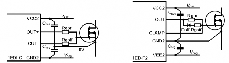
Click image to enlarge
Figure 2a & 2b. Implementing separate turn-on and turn-off gate resistance values for unwanted turn-on avoidance. Source Infineon AN2017-04
Separate RGON and RGOFF circuits can be implemented for each MOSFET. Figure 2 shows how this can be done using two types of drivers from Infineon’s EiceDRIVER family. The 1EDI-C driver on the left has separate source/sink outputs, while the schematic on the right shows a driver from the 1ED-F2 family that has a single output with negative turn-off voltage capability.
In an application note about fine-tuning SiC MOSFET gate drivers, STMicroelectronics recommends making RGON at least 1.5 times RGOFF, with resistance values of about 4.7Ω and 2.2Ω respectively.
There are also other desirable driver features to consider, including close delay matching, fast desaturation protection, under-voltage lockout, optimum circuit layout and an active Miller clamp. Read more about these additional features in the expanded version of this articleavailable on RS Components’ DesignSparkonline engineering community. DesignSpark’s Ask the Expert video series also features an informative Q&Aon SiC power devices with Christian Felgemacher from Rohm Semiconductor.
Conclusion
Controlling SiC MOSFETs at high switching speeds requires careful management of gate current and, ideally, asymmetrical gate-drive voltage (VGS) up to 15V to 20V for turn-on and -4V to -5V for turn-off. VGS of 0V may be acceptable in single-switch topologies, to save the extra complexity of generating a negative voltage for turn-off.
In any case, preventing spurious turn-on resulting from dVDS/dt transients or unintended gate currents is one of the most important aspects of designing the driver. A number of techniques can be considered, including optimizing the MOSFET gate-source threshold voltage through device selection, applying negative turn-off voltage, managing the relationship between high-side/low-side turn-on/turn-off gate resistors, or clamping the gate to a low voltage to actively hold the MOSFET off.
Gate-driver ICs optimized for SiC applications are in the market now. These not only support various ways of preventing unwanted turn-off, but also incorporate important safety features like fast desaturation protection, which is difficult to design using discrete components.