Silent Switcher 2 Regulator for SoC, Microprocessor Apps
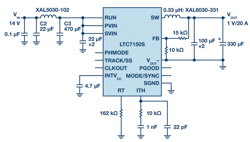
Figure 1. VIN = 14 V, VOUT = 1 V, 20 A. fSW = 400 kHz.
Power budgets continually rise for advanced SoC (system on chip) solutions used in industrial and automotive systems. Each successive SoC generation adds power hungry devices and increases data processing speed. These devices require reliable power, including 0.8 V for cores, 1.2 V, and 1.1 V for DDR3 and LPDDR4, and 5 V, 3.3 V, and 1.8 V for peripheral and auxiliary components. Moreover, advanced SoC solutions require higher performance than traditional PWM controllers and MOSFETs can provide. As a result, the solutions necessary must be more compact, with higher current capability, higher efficiency, and, more importantly, superior EMI performance. This is where our Power by Linear monolithic Silent Switcher 2 buck regulators can satisfy advanced SoC power budgets whilemeeting SoC size and thermal constraints.
20 A Solution from 20 V Input for an SoC
The LTC7150S raises the bar for high performance in industrial and automotive power supplies. It features high efficiency, a small form factor, and low EMI. Integrated high performance MOSFETs and thermal management features enable reliable and continuous delivery of currents up to 20 A from input voltages up to 20 V without heat sinking or airflow, making the LTC7150S ideal for SoC solutions, FPGAs, DSPs, GPUs, andmicroprocessors in industrial, transportation, and automotive applications.
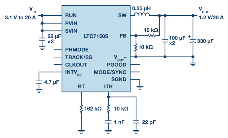
Figure 1a & Figure 1b shows a 1.2 V output at 20 A solution for SoC and CPU power using the LTC7150S switching at 1 MHz. This circuit can be easily modified to accommodate other output combinations, including 3.3 V, 1.8 V, 1.1 V, and 0.6 V to take advantage of the wide input range of the LTC7150S. The LTC7150S has the output current capability to act as a first stage 5 V supply, which can be followed by a number of downstream second-stage switching or LDO regulators at various outputs.
Click image to enlarge
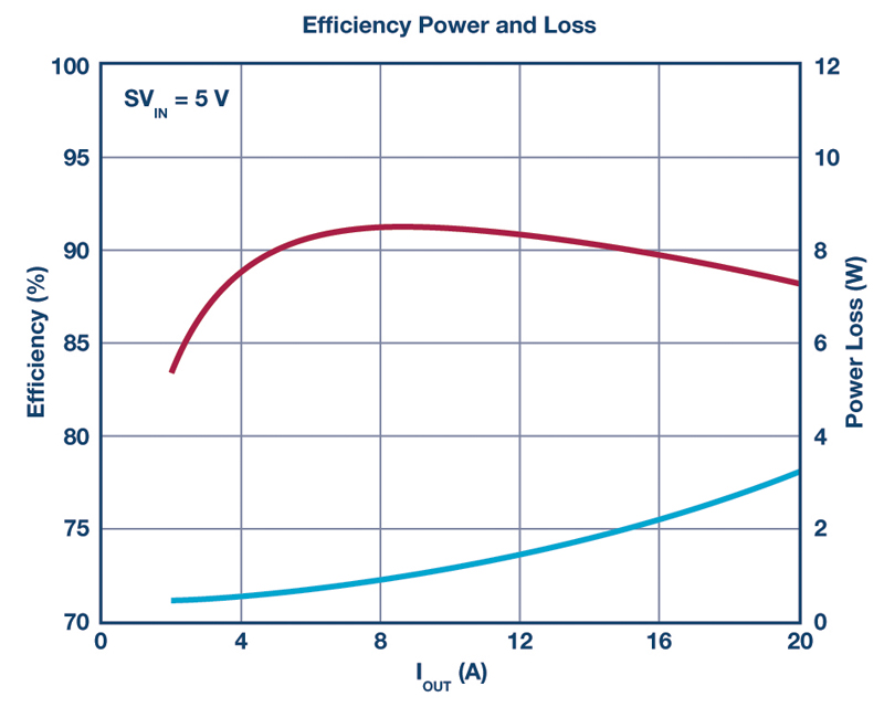
Figure 2. Schematic and efficiency of the buck converter: 12 VINto 1.2 VOUT at 20 A.
Silent Switcher 2 with Excellent EMI Performance
Passing EMI regulations at high currents typically involves a complicateddesign and test challenge, including numerous trade-offs in solution size, efficiency, reliability, and complexity. Traditional approaches control EMI by slowing down the MOSFET switching edge rates and/or lowering switching frequency. Both of these strategies come with trade-offs, such as reduced efficiency, increased minimum on- and off-times, and a larger solution size. Alternative mitigation techniques, such as a complicated bulky EMI filter or metal shielding, add significant costs in board space, components, and assembly, while complicating thermal management and testing.
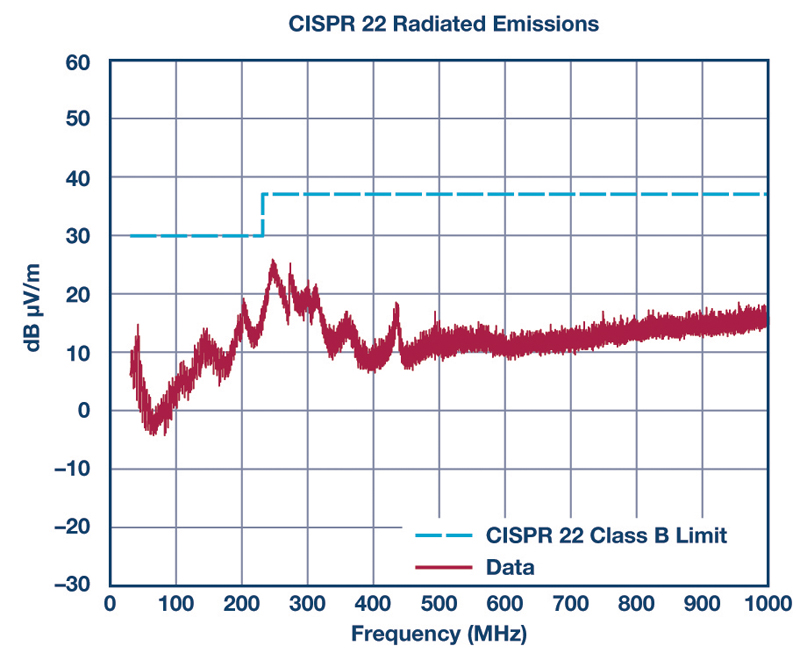
Analog Devices’ proprietary Silent Switcher 2 architecture self-cancels EMI via integrated hot loop capacitors, which minimizes noisy antenna size. This, combined with integrated MOSFETs, significantly reduces switching node ringing and associated energy stored in the hot loop, even with very fast switching edges. The result is exceptional EMI performance while minimizing the ac switching losses. Silent Switcher 2 technology is incorporated in the LTC7150S to minimize EMI and deliver high efficiency, which greatly simplifies EMI filter design and layout, ideal for noise-sensitive environments. LTC7150S passes the CISPR 22/CISPR 32 conducted and radiated EMI peak limits with only a simple EMI filter in front. Figure 3 shows the radiated EMI CISPR 22 test result.
Click image to enlarge
Figure 3. The radiated EMI performance of Figure 2.
High Frequency, High Efficiency Fits Tight Space
Integrated MOSFETS, integrated hot loop decoupling capacitors, built-in compensation circuits—all take the design complexity out of the systemand minimize total solution size with circuitry simplicity and Silent Switcher architecture.
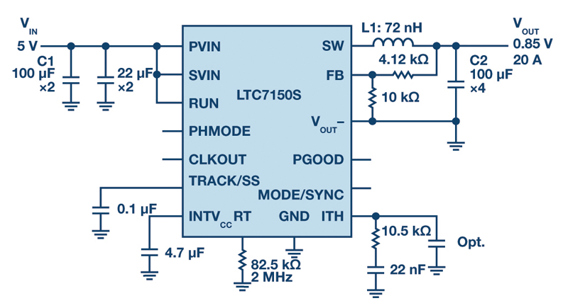
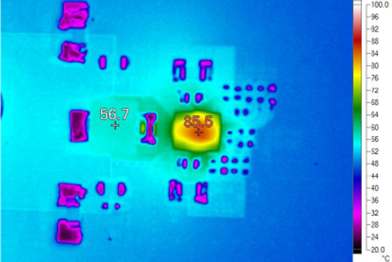
Thanks to high performance power conversion, LTC7150S delivers high current without the need for additional heat sinks or airflow. Unlike most solutions, both low EMI and high efficiency can be achieved at high frequency operation, ensuring a small passive component size. Figure 4a & Figure 4b shows a 2 MHz solution that uses a small 72 nH inductor and ceramic capacitors in a very low profile solution for FPGA and microprocessor applications.
Click image to enlarge
Figure 4. LTC7150S schematic and thermal image for 5 V input to 0.85 V/20 A output with fSW= 2 MHz.
Conclusion
The demand for more intelligence, automation, and sensing in industrial and automotive environments is resulting in a proliferation of electronic systems that require increasingly high performance power supplies. Low EMI has risen from an afterthought to a key power supply requirement—in addition to solution size, high efficiency, thermal efficiency, robustness, and ease of use. The LTC7150S meets stringent EMI demands in a compact footprint by incorporating Silent Switcher 2 technology. Integrated MOSFETs and thermal management features enable robust and reliable deliveryof currents up to 20 A continuously from input ranges up to 20 V, withswitching frequency ranges as high as 3 MHz.