Silicon Carbide Devices for Automotive Power Electronics
SiC technology and devices are becoming more mature with costs also coming down
Automotive OEMs and their suppliers have been on the high power, high growth vehicle electrification path for hybrid electric vehicles (HEVs)/electric vehicles (EVs) and beyond even to electrification of busses, trucks, trains and more electric aircraft (MEA). With high power demands beyond the efficiency and reliability that silicon IGBTs and MOSFET devices can offer, wide bandgap silicon carbide (SiC) solutions are on the cusp of huge growth within the transportation sector. Various market reports forecast growths to 40 percent CAGR after 2020, where SiC power discretes and module solutions are increasingly being adopted for mainstream automotive applications like DC-DC converter, external/onboard charger and powertrain traction control/motor drive.
SiC technology and devices are becoming more mature with costs also coming down with 6-inch wafer production. The quality and supply of wafers in the industry and the understanding of SiC devices by device engineers have evolved to the point where SiC products are more efficient and highly competitive (at the system level) when compared to silicon devices. SiC devices allow use of higher switching frequencies, resulting in more compact designs. SiC MOSFETs are inherently more efficient than IGBTs, the workhorse of power electronics, thus allowing use of smaller magnetics and heat sinks advantageous toward lower system size/weight/cost.
Some of the SiC benefits over silicon devices include:
· SiC MOSFETs and diodes both parallel easily. This is an advantage in high current modules like those used in traction drives. Figure 1 shows a normalized RDSon vs temperature with a 1200V MOSFET. The temperature dependence is less than that of silicon devices.
· SiC Schottky diodes are capable of operation in the multiple kV range in the tens of amps. The high bandgap means they do not have the high leakage like that of their lower voltage silicon devices.
· The body diode of SiC MOSFETs has a very fast recovery, roughly an order of magnitude faster than that of silicon devices.
· Due to the fast carrier recovery SiC MOSFETs tolerate extremely high slew rates. It is virtually impossible to damage a SiC MOSFET by exceeding its slew rate.
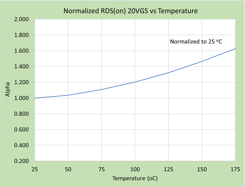
Click image to enlarge
Fig. 1: RDSon vs. Temperature of Mocrosemi’s NextGen 1.2 kV, 40 mohm SiC MOSFET (MSC040SMA120B).
SiC solutions targeting the higher reliability of automotive applications do face some challenges. SiC is fundamentally a different crystalline structure than silicon material. A SiC device of equal performance has a much smaller die, allowing more compact designs although this introduces challenges with heat flux density. SiC devices has some of the same failure modes as silicon devices and some unique failure modes. The transportation sector requires high reliability, and the need for these high levels of reliability has been why engineers have been slow to accept SiC devices. That’s now changing.
Automotive Standards
Automotive standard AEC-Q101 was developed around silicon devices and provides a high performance standard for the automotive environment that removes some of the ambiguity in conventional commercial data sheets by guaranteeing a level of testing to exact data sheet specifications. The AEC-Q101 specification is relatively light on long-term reliability testing, and the need for long-term reliability of SiC devices may introduce new qualification challenges. Also, some of the tests required by AEC-Q101 may be more of a challenge for SiC, which include:
· High temperature gate bias (HTGB) for 1,000 hours at 100 percent rated gate voltage. This is an important test with SiC. Fabrication of a stable SiC MOSFET gate has been one of the biggest challenges with SiC.
· High temperature reverse bias (HTRB) for 1,000 hours at 100 percent rate voltage. This also is a challenging test with SiC because of the gate stability. Currently this test is done with no gate bias but it is possible in the future it will change given that negative gate bias is generally used with SiC MOSFETs.
· Temperature cycle (TC) test generates surface stress on a device that can be a challenge with some gate structures.
Beyond AEC-Q101
Eventually testing beyond the current AEC-Q101 may be required. Microsemi has considered the following.
UIS
Unclamped inductive switching (UIS) is a test where a device is driven over voltage into breakdown. Most modern silicon devices can tolerate breakdown energies on the order of Joules. Defects within individual devices make it necessary to test all devices if a UIS rating is to be guaranteed. This is not generally done, which makes a UIS rating nice to have but not something to depend upon device to device. In this respect SiC is the same. A properly designed SiC device can tolerate UIS to the point that the die heats to its upper temperature limit.
Where SiC differs is that the UIS test may evolve into part of a test for long-term degradation of the device structure. A metric of degradation may evolve by first screening a population of devices with UIS, subjecting them to stress, and then again subjecting them to UIS. SiC devices have a 4H-SiC structure, which is complex, and may be related to this observation. If this is not incorporated into AEC-Q101, it still may become part of a test for high reliability devices.
RUIS
Repetitive unclamped inductive switching (RUIS) testing is used to measure the stability of a device over time when placed in a repetitive breakdown condition. Changes in MOSFET leakage and threshold or changes in diode leakage were common in the past. With the proper substrate and good design practice this is no longer an issue.
Microsemi uses RUIS as part of a test sequence to guarantee design margin in the gate. Testing with our next-generation SiC MOSFETs has shown there is no degradation of the gate or leakage after exposure to 10K RUIS pulses. Figure 2 shows a trigger, drain current and drain current in a 100mJ UIS event. The drain potential on the MSC040SM120 is 1.77KV during breakdown.
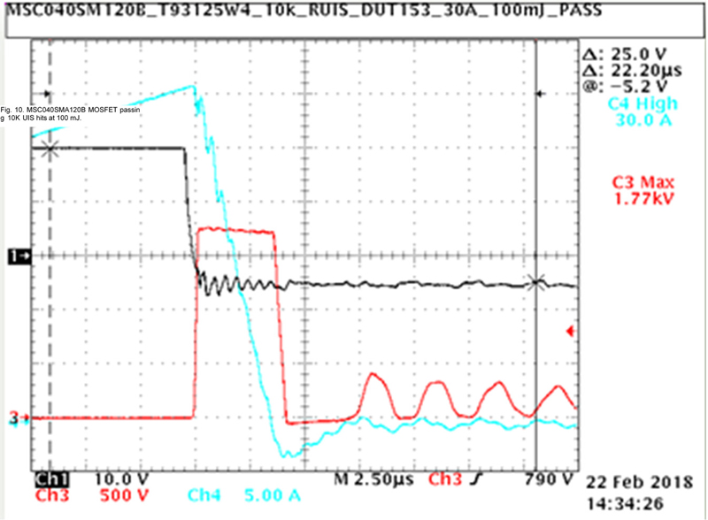
Click image to enlarge
Fig. 2: MSC040SMA120B MOSFET passing 10K UIS hits at 100 mJ.
High Stress Power Cycling
Microsemi device testing includes artificial aging by power cycling. MOSFETs can be artificially aged by power cycling devices over a wide temperature range. With a properly designed system the long-term reliability of a device can be assessed quickly. This is a test of a packaged device’s metallization, the die bond and the quality of the bond wire attach. SiC MOSFETs are proving to be almost as reliable as silicon devices. They have an odd characteristic that is more pronounced than with silicon devices. Over the lifetime of the device there is slight degradation of RDSon. This is common to all manufacturers at usually about 5 to 15 percent. A design margin should be considering with RDSon if this is of concern. In addition, this test has shown that the device surface structure may influence the lifetime. Vertical structure MOSFETs generally don’t do as well.
Rth
To gauge the lifetime expected from a device it is necessary to accurately measure the package thermal resistance. A SiC die is typically small relative to the back metal in a discrete device. This results in a high heat flux localized under the die and the back metal thermal interface presenting a higher thermal resistance than would be expected than with a calculation based upon the whole back metal area. This may be the reason for high variability of the margin between the actual device package thermal resistance and the specified resistance between manufacturers. Complicating this is discrete device designs usually require an insulating thermal interface. Most are very thin which presents a relatively high capacitance between the back metal and the heatsink. With discrete devices ceramic insulators may be considered. Modules do very well with integrated ceramic insulation.
SiC Supply
While the power electronics industry had to deal with short-term challenges of EPI substrate availability that affected both silicon and SiC device lead times, SiC products are over this supply hump as additional substrate vendors are coming online and high volume and mature SiC manufacturing are in place to support the ramp in automotive adoption of SiC solutions.
Summary
The benefits of SiC solutions over silicon IGBT and super junction MOSFET-based solutions are evident at the system level for efficiency and reliability at high power. Microsemi suggests going beyond what is only auto-qualified, and this should resonate well with automotive engineers. For more information on SiC solutions, please visit https://www.microsemi.com/product-directory/discretes/3613-silicon-carbide-sic.
Microsemi