Silicon Reinvented: Architectural Innovations Beyond SuperJunction Power MOSFETs

The semiconductor industry has been centered around silicon for decades. Silicon transistors and diodes have been commercially available since the 1950s and 1960s. Since this time, significant advances have typically emerged about once per decade
Figure 1: The evolution of semiconductor architectures from HEXFET (left) to SuperJunction (middle) and the latest SuperQ technology (right), with dielectric charge-balancing structure shown in red
In the 1970s, the 1D power MOSFET, aka HEXFET™, was introduced. The 1980s saw the launch of the IGBT, and in the 1990s, reduced surface field (RESURF) devices – aka SuperJunction™ devices were introduced.
Over the last two decades, improvements in silicon power devices have been largely evolutionary rather than revolutionary, while much of the industry’s research focus has shifted toward wide-bandgap materials such as silicon carbide (SiC) and gallium nitride (GaN).
Despite this shift in research emphasis, approximately 89% of global spending on power semiconductors remains allocated to silicon technologies. Due to the significantly lower cost of silicon MOSFETs compared with alternative materials, this corresponds to approximately 95% of all device shipments.
Silicon retains this dominant position due to its manufacturing maturity, cost advantages, robustness, and well-understood material properties. However, without further architectural innovation, silicon devices risk being displaced in applications where efficiency, power density, or switching performance are critical.
This article examines a newly commercialized asymmetrical RESURF architecture (aka SuperQ™) and compares its performance against SuperJunction-type devices across multiple figures-of-merit.
Evolution of Silicon Power Device Architectures
The HEXFET MOSFET, introduced in 1979, used all the silicon area for conduction. This resulted in the core problem that its on-resistance scales with the breakdown voltage to the power of 2.5 (BV2.5), limiting device performance and usefulness in high-voltage applications.
SuperJunction technologies, introduced in the late 1990s, addressed this limitation by employing two-dimensional charge balancing. This is accomplished by introducing alternating p-type and n-type vertical pillars in the drift region, where the p-pillars laterally deplete the n-pillars under reverse bias, allowing much higher doping without sacrificing breakdown voltage.This approach enabled higher breakdown voltages while achieving near-linear scaling of on-resistance with voltage rating.
To achieve this, however, the conduction region was reduced to 50% of the die, with the p-regions supporting the blocking function. While this represented a major advancement at the time, further refinement of SuperJunction structures became increasingly complex and expensive. At this point, many believed that silicon had reached (or was fast approaching) its end and openly speculated that other materials would be the future. However, continued innovation at the architectural level suggests that silicon performance limits are not yet reached.
SuperQ continues to use a RESURF structure but introduces an asymmetrical configuration that significantly widens the n-channel region. The conventional p-pillar is replaced with a high-aspect-ratio trench that incorporates dielectric sidewall charge, enabling voltage blocking while maximizing the conduction area.
Compared with the epitaxial growth and implant processes used in SuperJunction devices, the SuperQ architecture employs a simplified process flow while achieving voltage blocking levels of approximately 19–20 V/µm with thinner epitaxial layers. These voltage-blocking levels represent an approximate 33% increase over those of their SuperJunction counterparts. This higher blocking level enables higher allowable doping concentrations, which further reduce conduction losses.
As a result, SuperQ achieves approximately a 2.6× improvement in RSP relative to conventional silicon devices and remains compatible with CMOS manufacturing on 200-mm and 300-mm wafers. The architecture is also applicable to other device types, including diodes, IGBTs, and integrated power ICs, at voltage ratings extending toward 1.2 kV.
What is SuperQ?
SuperQ is a Power MOSFET architecture based on an asymmetrical RESURF structure that significantly increases the available n-type conduction region compared with conventional SuperJunction devices. Unlike SuperJunction technologies, which use a roughly symmetrical RESURF structure with an approximate n-conductive region of 50%, the SuperQ architecture can almost completely eliminate the p-pillars. This is achieved through etching and atomic layer deposition and the implementation of a novel charge-balancing structure from dielectric materials, creating a structure with an n-conduction region leverages up to 95% of the available area, as shown in Figure 1.
The increase in available conduction area directly reduces the specific on-resistance per unit area (RSP), enabling higher performance within a given die size and package footprint.
Performance Comparison
The first SuperQ-based MOSFETs were launched in 2025, with 150V and 200V devices either in mass production or sampling. Additionally, 300V and 400V MOSFETs are in development.
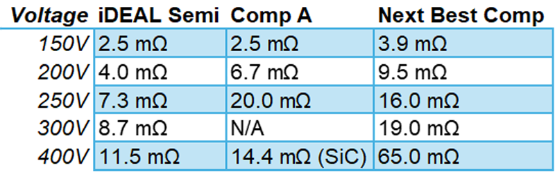
As an example, two 150V SuperQ devices (iS15M2R5S1T and iS15M2R5S1H) have on-resistance (RDS(on)) values of just 2.5mΩ when packaged in TOLL and D2PAK-7L. This performance is comparable to the lowest on-resistance values currently available in commercially released SuperJunction devices, while the next closest competitor exhibits more than 50% higher resistance.
At higher voltages, the performance advantage increases. At 200V, a SuperQ device in a TOLL package achieves 4.0mΩ, compared with 6.7mΩ for the closest competing silicon device and 9.5mΩ for the next alternative.
The following table summarizes representative minimum RDS(on) values for similarly packaged devices at room temperature, based on published datasheets.
Click image to enlarge
Table 1: An RDSon comparison of SuperQ MOSFETs with the leading two directly comparable devices in each voltage range
Provisional data for the upcoming 400V SuperQ devices indicates an RDS(on) of approximately 11.5mΩ, compared with approximately 65mΩ for the best available silicon alternative.
Switching Performance and Dynamic Losses
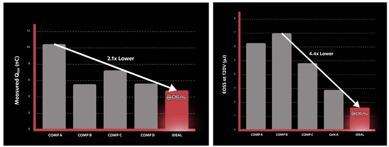
In modern high-frequency power conversion applications, conduction losses account for only a portion of the total device loss. Switching charge (QSW) becomes increasingly important as switching frequency rises. This presents challenges when designing ultra-compact power solutions with high levels of power density.
Click image to enlarge
Figure 2: SuperQ significantly reduces switching charge and total capacitive energy storage
Measured data indicates that SuperQ devices can reduce switching-related losses by approximately 50% compared with similarly rated silicon MOSFETs. This enables designers either to reduce losses at a given switching frequency or to increase operating frequency while maintaining similar thermal performance. Higher switching frequencies also allow the use of smaller passive components, increasing overall power density.
A further performance advantage of SuperQ is the reduced energy stored in the device’s output capacitance (COSS). Compared to some equivalent silicon devices on the market, the capacitive energy stored (EOSS) is less than a quarter, dramatically improving performance in higher frequency designs.
In addition to efficiency gains, the SuperQ architecture delivers significantly improved short-circuit withstand current (SCWC). The expanded n-type conduction region and reduced current crowding enable higher peak fault currents and longer fault survival times, providing designers with greater protection margins during shoot-through and abnormal operating events.
Reliability and Qualification
Devices are fully production-screened for unclamped inductive switching (UIS) and characterized across safe operating area limits. Qualification includes JEDEC reliability testing such as HTRB, HTGB, thermal cycling, and humidity stress, with junction temperature ratings up to 175 °C.
Initial SuperQ devices have also completed AEC-Q101 automotive qualification, supporting use in automotive, industrial, and data-center power applications that require long-term reliability.
Cost, Manufacturing, and Supply Chain Considerations
SuperQ is material-agnostic and can be applied to silicon as well as to alternative semiconductor materials. The architecture applies to discrete MOSFETs, diodes, IGBTs, and integrated power ICs.
While similar performance improvements may be achieved using wide-bandgap devices, SuperQ MOSFETs can be adopted without changes to gate-drive voltage levels, drivers, or power topologies. Because SuperQ remains a silicon-based architecture, it maintains compatibility with existing design practices and manufacturing infrastructure.
With over 95% of semiconductor manufacturing still firmly entrenched in silicon, the move to alternative materials can be costly, time-consuming, and somewhat risky. SuperQ devices can be produced in existing fabs using established equipment and process flows. This minimizes supply-chain disruption while supporting high yield and cost efficiency.
Roadmap and Outlook
With the first devices in production, the SuperQ architecture demonstrates a viable path for extending silicon power device performance. Additional devices are in development, including MOSFETs with breakdown voltages beyond 650 V, as well as integrated solutions such as half-bridges and dual MOSFETs.
Although silicon power device performance has appeared to plateau since the late 1990s, these limitations have largely been architectural rather than material-based. SuperQ illustrates that architectural re-engineering can continue to extend the performance envelope of silicon devices, enabling higher efficiency and power density while preserving the cost, supply-chain stability, and design familiarity of silicon technology.