Advances in technology are enabling a general reduction in semiconductor feature size
The die area of power transistors is effectively dictated by their power rating. For a given thermal dissipation, smaller just means higher junction temperatures and potential reduction in reliability, especially with power cycling. For that reason, minimizing the thermal resistance from die to case and ambient is key.
Thermal resistance at the chip level
A power device die in a technology such as silicon carbide (SiC) must remain within its safe operating area and keep junction temperatures below 175°C. Figure 1 shows the typical mechanical arrangement and heat flow path.

Click image to enlarge
Figure 1a and 1b: Solid model of a surface mount semiconductor device (1a) with the packaging components soldered to an insulated metal substrate and (1b), the thermal model in ANSYS showing heat flow from the die to the environment
The total thermal resistance from die to ambient is the sum of the individual thermal resistances of each material in the path. Generally, Integrated Device Manufacturers (IDMs) design their devices to have a predictable, reproducible, junction-to-case thermal resistance (RθJC). This figure comprises the thermal resistance of the semiconductor substrate, the material used to attach the die to the package, and the package material itself.
In power devices based on a silicon substrate, the die is typically soldered to the (normally copper) package, Figure 2.
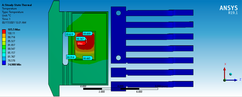
Click image to enlarge
Figure 2a, 2b and 2c: Thermal model of a typical power semiconductor, 7L D2PAK, showing the different temperature gradients from chip to case. Side cross section view (2a), temperature probing at different points on the die top (Tj) (2b) and temperature probing at different points on case (Tc) (2c)

Click image to enlarge
Table 1: Material properties and calculated RθJC from Figure 2
Although smaller die can perform better dynamically and a given wafer size can yield more, a bigger die offers a larger surface area for the heat to flow away from as it leaves the junction, resulting in a lower junction temperature. It is vital therefore to achieve the lowest RθJC practical to enable smaller die to be used.
Silver sintering reduces thermal resistance
After the junction and die, the next thermal barrier to heat flow is the interface between die and package. The industry standard is to use solder attachment and mostly, this is a good choice, as it is easy to work with, relatively cheap and relatively reliable. The thermal conductivity of this interface depends on the volume of the material, not just its thickness because heat spreads in all directions but at different rates, based on the resistance it encounters. One alternative to soldering using a lead-based alloy is to use a paste capable of being sintered. These materials tend to have a much higher thermal conductivity and can often be applied in thinner layers. Silver is a good example, with sintered layers achieving a thermal conductivity of 140-200 W/(m⋅K). This compares favourably with lead-based solder with a thermal conductivity of just 25 W/(m⋅K) (Table 2).
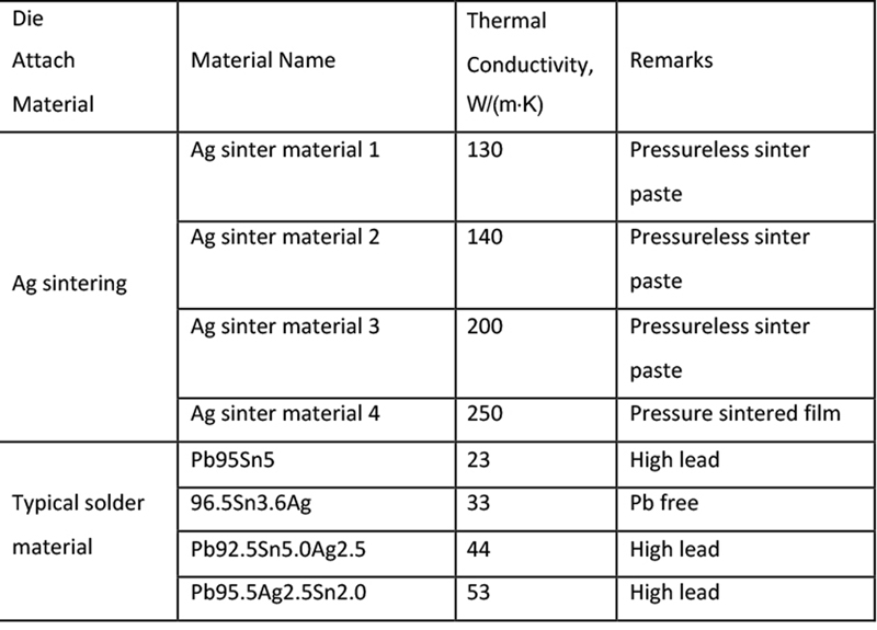
Click image to enlarge
Table 2: Thermal conductivity of silver sinter and solder processes
Silver sintering – the rationale
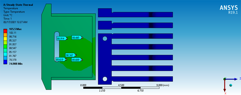
In power devices, with high heat flow through the solder attach, more emphasis needs to be put on the thermal performance of the interface and its ability to handle high temperatures without degrading. Replacing the solder with sintered silver, with its much lower thermal resistance, improves RθJC and, thanks to its higher melting point, also adds thermal margin to the overall design (Figure 3).
Click image to enlarge
Figure 3a and 3b: Thermal model of 7L D2PAK showing the different temperature gradients from chip to case using Pb95.5Ag2.5Sn2.0 solder die attach (3a), and using 140W/(m⋅K)Ag sinter die attach (3b). The latter achieves a 28% reduction in thermal resistance
Engineers may not have been aware that silver sintering is an option in power semiconductors, with the consequent better thermal margin and added flexibility in heat management, but the technique is becoming mainstream for high-performance devices. As outlined earlier, smaller die area comes with advantages in terms of performance and cost, but disadvantages in terms of heat dissipation. Choosing silicon carbide (SiC) devices means the advantages are still present, but the disadvantages are less pronounced. This is one of the main reasons why the semiconductor industry and all of the vertical markets it supports are so interested in SiC-based power semiconductors.
The combination of a SiC substrate – which is both smaller and thinner than a silicon substrate – coupled with using sintered silver as the die attach, produces a RθJC figure that is comparable to other power semiconductors, but with the advantages of SiC. These include higher switching speeds and higher efficiency, leading to greater thermal density and, in turn, smaller and lower cost end-products.
Not all IDMs need to use sintered silver
With such clear benefits, why are all IDMs not using sintered silver? This is mostly because silicon-based power devices, like IGBTs, have a large die area and therefore anyway have good RθJC and sintered silver would provide less benefit. As alluded to earlier, the thermal resistance between the case and ambient, RθCA – which is largely dictated by the PCB and system design, and therefore not under the control of the IDM – is normally much more significant than the thermal resistance between the junction and the case, RθJC. This is true for all semiconductors, not just power devices.
For a power semiconductor that does have a comparatively small die area, typical with a SiC device, the smaller die effectively dictates the use of silver sintering rather than lead-based solder. The higher thermal conductivity offered by sintered silver ensures the device can still operate within its safe operating area, maintaining junction temperature below its operating maximum, even though the thermal path from the die has much smaller area.
Reasons why engineers should like sintered silver
Typically, manufacturers of silicon-based power semiconductors are unlikely to change to sintered silver in place of solder. However, while the benefits it brings to SiC devices are largely related to their higher performance and smaller die size, it actually has significant advantages to system engineers generally.
Firstly, an interface with a higher melting point introduces greater thermal margin in a design. As the junction heats and the thermal path becomes more critical in a silicon/solder-based device, the solder could approach its melting point. This would not necessarily cause sudden failure, but repeated power cycling will stress and degrade the interface.
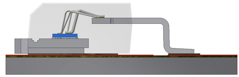
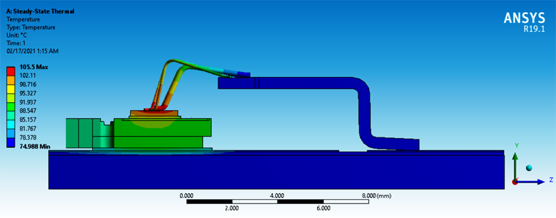
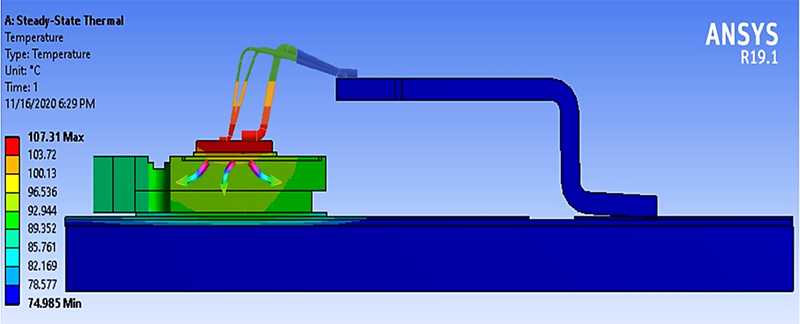
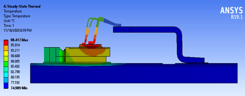
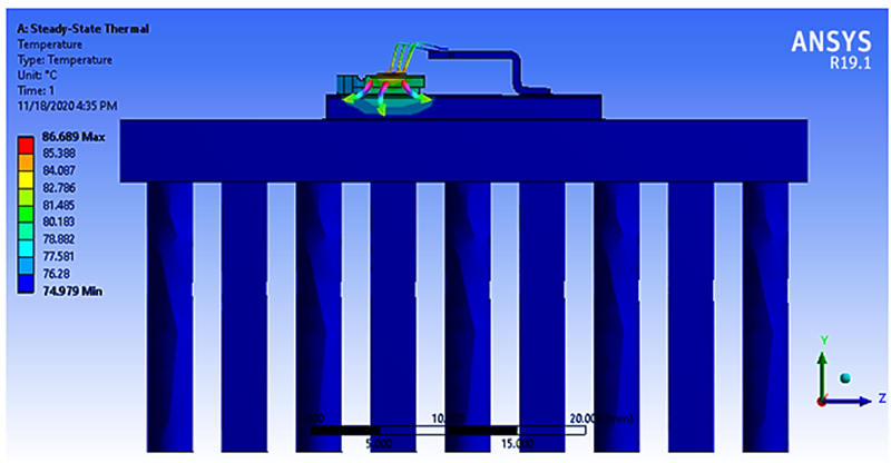
More positively, the use of sintered silver can actually be an agent for wider system gains. As mentioned above, the thermal resistance between the case and ambient, RθCA, is typically the dominant figure in the total thermal path. However, the continued development of more sophisticated and efficient heat-sinking solutions, such as liquid cooling in high-performance applications, shifts the focus back onto the device RθJC for best overall system performance (Figure 4).
Click image to enlarge
Figure 4a and 4b: 3D model of a 7L D2PAK power device showing the package soldered on an insulated metal substrate and mounted on a heatsink (4a) and thermal simulation (4b) showing that lower junction temperature (Tj) can be achieved with more efficient cooling
Conclusion
Knowing that silver sintering die-attach gives wider performance benefits and value can be a useful insight. UnitedSiC is leading the industry in the process of making silver sintering standard in all of its silicon carbide power semiconductor products.
Engineers interested in learning more should contact their local UnitedSiC FAE.