Simple and cost effective dimming solutions

Simple and cost effective dimming solutions
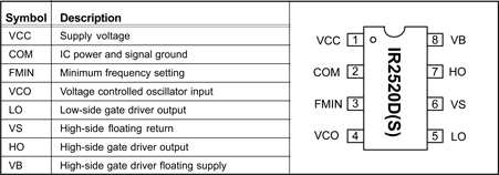
Dimming of fluorescent lamps will normally require the incorporation of a complex, high pin count controller IC into the circuit design. As a result, dimming circuits are more difficult to create than non-dimming alternatives, needing a larger number of components, taking up more board space, and raising the system's total price tag. These issues are compounded still further when considering compact fluorescent lamps, due to the small form factors involved and the need to be highly cost effective. Here we look at a non-dimming ballast control based on an 8-pin controller IC and explain how dimming functionality can be added without needing to increase the pin count. With an existing 8-pin, non-dimming lighting ballast controller (for example, the IR2520D from International Rectifier, shown in Figures 1 and 2) only two pins are used (FMIN and VCO) to deal with preheat, ignition and running requirements of the fluorescent lamp. The remaining pins perform standard functions such as IC supply and ground (pins VCC and COM), plus high- and low-side gate drive for the half-bridge (pins LO, VS, HO and VB).
Within a non-dimming ballast circuit, current charges the VCC until it reaches the internal UVLO+ threshold. When VCC goes past this threshold, the IR2520D enters frequency sweep mode, the gate driver outputs (LO and HO) and the half-bridge circuit then starts oscillating at the maximum frequency. The charge-pump circuit then becomes the main supply circuit for the IC, maintaining the VCC at the internal clamp voltage. A small internal current source at the VCO pin slowly charges up an external capacitor causing the voltage on the VCO pin to ramp up linearly. This in turn ramp downs the frequency of the gate driver outputs (LO and HO), and the half-bridge switching circuit from its maximum starting value. The lamp voltage increases as the frequency ramps down towards the resonance frequency of the high-Q, under-damped output stage. The VCO pin voltage continues to increase and the frequency keeps decreasing until the lamp ignites. The output circuit then becomes an over-damped, low-Q circuit. The VCO voltage increases, causing the IC to enter run mode. The frequency level stops decreasing once the VCO pin surpasses 5V and stays at the minimum frequency as programmed by an external resistor on the FMIN pin. With demand for dimming functionality becoming ever greater, but engineers not wanting to sacrifice the advantages of compact low pin count devices like the IR2520D, a way to control dimming through the pins already available needed to be found. As the VCO pin is required to perform the necessary frequency sweep for preheat and ignition, the FMIN pin was left as the only viable option through which this could be accomplished.
The dimming of a fluorescent lamp can be achieved by using operating frequency to control the current being applied to the lamp. As the frequency of the half-bridge is increased, the gain of the resonant tank circuit decreases and the lamp current lowers. It is possible to regulate the lamp current to a dimming reference level by continuously adjusting the half-bridge frequency through closed-loop feedback circuit. Dimming is enabled by combining the AC lamp current measurement with a DC reference voltage at a single node. The AC lamp current is measured across sensing resistor RCS and coupled onto the DC dimming reference via feedback capacitor CFB and resistor RFB. The feedback circuit regulates the valley of the AC+DC signal to COM as the DC dimming level is raised or lowered by continuously adjusting the half-bridge frequency. This causes the amplitude of the lamp current to then increase or decrease so that dimming can be carried out. If the DC reference is increased, the valley of the AC+DC signal will rise above COM and the feedback circuit will lower the frequency in order to enlarge the gain of the resonant tank. This will raise the lamp current, as well as the amplitude of the AC+DC signal at the DIM pin, until the valley reaches COM again. If the DC reference is decreased, the valley will decrease below COM. The feedback circuit will then increase the frequency to lower the resonant tank gain until the valley reaches COM again. The IR2520D's FMIN pin, used to program a single running frequency, has now been replaced with a DIM pin, which measures the AC+DC signal for dimming. The IRS2530D dimming control IC offers a complete 8-pin solution that contains all dimming ballast functions. The VCO pin includes the frequency sweep timing control for preheat and ignition, and also programs the loop speed for the dimming feedback circuit during dim mode. When a voltage is first applied to VCC (14V, typical) the IC exits UVLO mode and enters preheat/ignition mode. The half-bridge begins oscillating at the maximum frequency and the internal current source at the VCO pin begins charging up an external capacitor (CVCO) linearly from COM. The output frequency decreases as the VCO voltage increases and the lamp filaments are preheated by secondary windings from the resonant tank inductor. As the VCO voltage charges up, the frequency decreases towards the resonance frequency of the resonant tank circuit and the output voltage across the lamp increases. The lamp ignites when the output voltage exceeds the lamp ignition threshold voltage, lamp current begins to flow, and the IC enters dim mode. A schematic showing a complete dimming mini-ballast circuit is described in Figure 3. It is designed to run from a 220VAC line and to drive a 25W compact fluorescent lamp. The 220VAC/50Hz line input voltage is full-wave rectified (BR1) and then goes through the EMI filter (CF and LF) before being smoothed by the DC bus capacitor (CBUS). The half-bridge switches (MHS and MLS), which are controlled by the IRS2530D, allow preheating, igniting and dimming of the lamp. RVCC1 and RVCC2 provide the micro-power start-up current for the IC's VCC supply, and the charge pump (CSNUB, DCP1 and DCP2) takes over as the IC supply once the half-bridge begins to oscillate. The resonant tank circuit (LRES and CRES) provides the transfer function for generating the high voltages needed for lamp ignition and low-pass filtering for dimming. Secondary windings from the resonant inductor (LRES: A, B) are used to heat the filaments of the lamp during preheat and dimming, and also separate the lamp current from the filament current allowing for a single current-sensing resistor (RCS) to be utilized for sensing the lamp current. The AC lamp current measurement across RCS is coupled to the DIM pin through a feedback capacitor and resistor (CFB and RFB). A potentiometer dimming input circuit is used (PDIM, RMIN, RMAX) to convert the potentiometer resistance to the dimming reference voltage for the IRS2530D through the DIM pin. Protection against ballast fault conditions (failure to strike, open filament, and low AC line/brown-out) are incorporated into the IRS2530D to further reduce component count.

There is a clear need for simple and cost effective dimming solutions which take up the minimum of real estate and do not require a large number of components. The 8-pin IRS2530D offers the means to develop dimming circuits in a quick and unproblematic manner. Furthermore, it has the potential to bring dimming features to a broader spectrum of applications, thus allowing marked energy savings to be realized. www.irf.com