Simple Power Backup Supply for a 3.3 V Rail
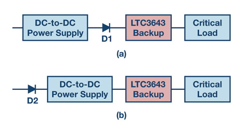
Figure 1(a) and (b). Location of the blocking diode in the backup system schematic.
Data loss is a concern in telecom, industrial, and automotive applications where embedded systems require a dependable supply of power. Sudden power interruptions can corrupt data during read and write operations performed by hard drives and flash memory. Designers often use batteries, capacitors, and supercapacitors to store enough energy to support critical loads for a short time during a power interruption.
The LTC3643 power backup supply allows designers to use a relatively inexpensive storage component: low cost electrolytic capacitors. In the backup or holdup supply presented here, the LTC3643 charges a storage capacitor to 40 V when power is present and discharges it to the critical load when power is interrupted. The load (output) voltage can be programmed to any voltage between 3 V and 17 V.
The LTC3643 easily fits backup solutions for 5 V and 12 V rails, but a 3.3 V rail solution requires extra care. The minimum operating voltageof the LTC3643 is 3 V, which is relatively close to the nominal 3.3 V input voltage level. This is too tight when a blocking diode is used to decouple the backup voltage source from noncritical circuitry, as shown in Figure 1a. If D1 is a Schottky diode, its forward voltage drop—as a function of load current and temperature—can reach 0.4 V to 0.5 V, enough to place the voltage at the LTC3643 VIN pin below the 3 V minimum. As a result, the backup supply circuit may not start up.
One possible solution is to move the diode to the input of the supplying dc-to-dc converter, D2, as shown in Figure 1b. Unfortunately, in this scenario, noncritical loads connected to the upstream dc-to-dc supply can draw power from the backup supply and leave less energy for critical loads.
3.3 V Backup Supply Operation
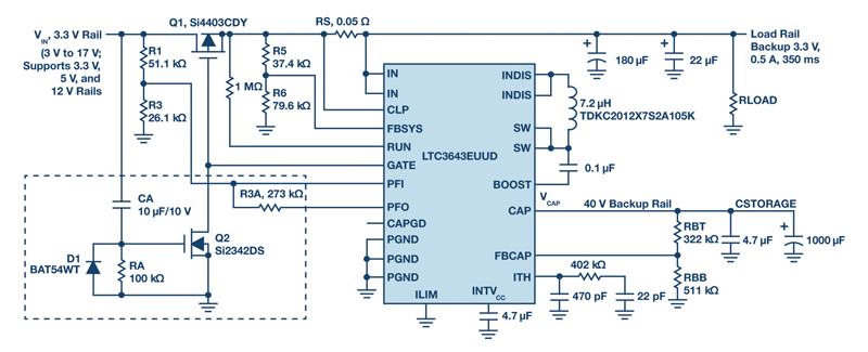
Figure 2 shows a solution to producing a 3.3 V backup supply that reservesenergy for critical loads using a blocking MOSFET. The blocking diode shown in Figure 1 is replaced by Q1, a low gate threshold voltage power P-channel MOSFET.
The key to operating the backup supply in a 3.3 V environment is the addition of the series RA-CA circuit. At startup, as the input voltage rises, thecurrent through the capacitor CA is governed by the equation ICA= C × (dV/dt).This current generates a potential across RA, which is enough to enhance Q2, a low gate threshold voltage small signal N-channel MOSFET. As Q2 turns on, it pulls the gate of the Q1 to ground, providing an extremely low resistance path from the input voltage to the supply pins VINof LTC3643. Once 3.3 V is applied to the converter, it starts up, pulling down both the gate of Q1 and the PFO pin, and it starts charging the storage capacitor.
Click image to enlarge
Figure 2. Enhanced schematic of the LTC3643 solution for a 3.3 V rail.
As the 3.3 V rail reaches steady state, the ICAcurrent reduces to the point where the voltage across RA falls below the Q2 gate threshold level and Q2 turns off, no longer affecting the functionality of the backup converter.Also, the PFO pin grounds R3A, which resets the PFI pin power fail voltage level to the minimum 3 V to ensure that the converter remainsoperational when the input voltage source is disconnected.
Circuit Functionality
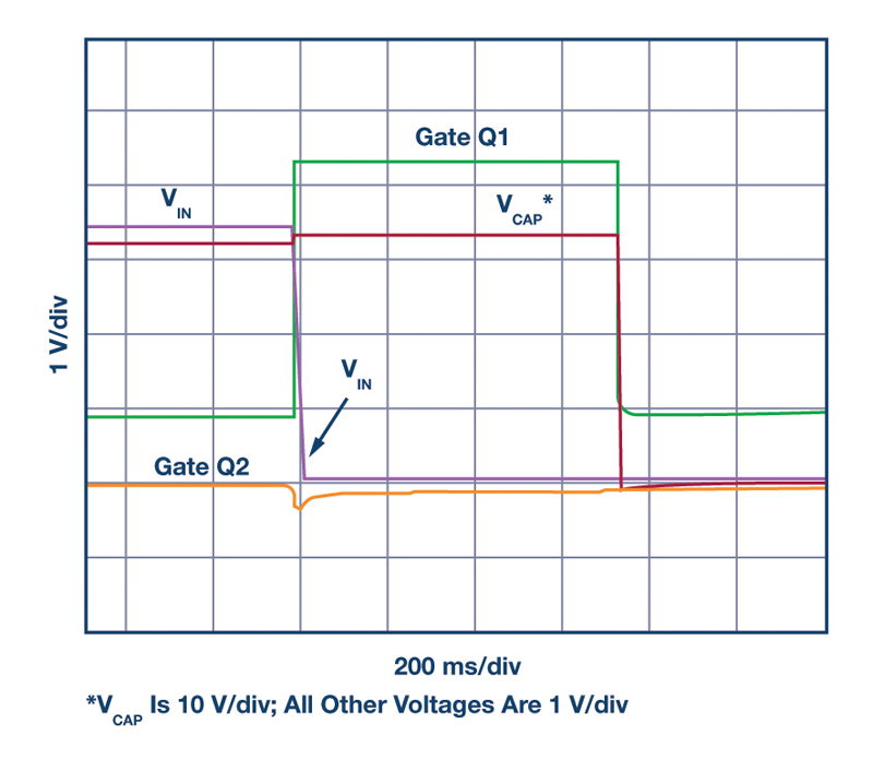
The waveforms in Figure 3 show results as the 3.3 V rail starts up. As the input voltage rises, so does the gate of Q2, pulling the gate of Q1 low. Q1 remains enhanced, allowing the full 3.3 V to reach the LTC3643,bypassing the Q1 body diode. Eventually the gate of Q2 voltage drops below the threshold level and Q2 turns off—by this time the LTC3643 is fully operational and takes control over the gate of Q1.
The versatility of the LTC3643 is on display here: specifically, its ability to limit the charging current of the boost converter used to charge the storage capacitor. In cases where total current must be minimized, such as when there are long lines or high impedance voltage sources, the boostcurrent can be set relatively low in order to minimize the effect of chargingcurrent on the input voltage drop. This is particularly important for 3.3 V rails. In Figure 2, the 0.05 Ω resistor RS sets a limit of 0.5 A (10.5 A load)for the boost converter charging the current (the maximum possible set limitis 2 A); the rest is delivered to the load.

Click image to enlarge
Figure 3. Waveforms of 3.3 V rail for power-up.
Figure 4 shows the waveforms when the 3.3 V rail is lost. As the input voltage falls, the voltage at the gate of Q2 remains unchanged, close to ground, and Q2 remains off. In contrast, the voltage at the gate of Q1 rises sharply to 3.3 V. This turns Q1 off, with the body diode of Q1 actingas a blocking diode, which decouples the load from the input. At this point, the backup supply takes over, with the LTC3643 supplying 3.3 V to the criticalload by discharging a storage capacitor.
Click image to enlarge
Figure 4. Waveforms of 3.3 V rail for power-down.
Conclusion
The circuit presented here enables the LTC3643 to be used as abackup supply solution for 3.3 V rails. The LTC3643 simplifies backup supplies by employing low cost electrolytic capacitors as the energy storage component.