Simplifying Design of Analog Input Modules for Process Control
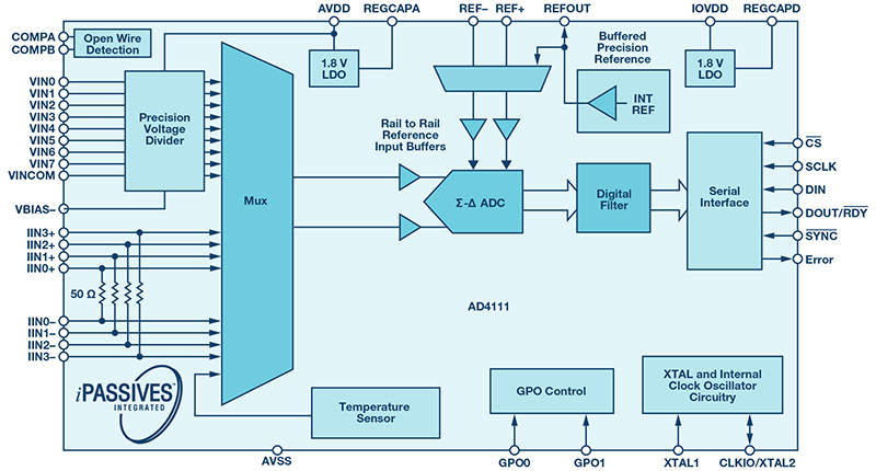
Figure 1. AD4111 functional block diagram
When designing analog input modules for process control applications such as programmable logic controller (PLC) or distributed control system (DCS) modules, the main trade-off considered is usually performance vs. cost. A tradition exists in this application space of using bipolar ±15V rails to supply active front-end components that are used to attenuate or gain input signals. This impacts the cost of bill of materials (BOM), as well as adding to the complexity of the design with the creation of the isolated bipolar supplies. To save on costs, an alternative approach is to architect with a single 5V supply. The single 5V rail greatly reduces the complexity of the design of the isolated supply for the analog front ends. However, it can introduce other pain points and may result in a lower accuracy measurement solution. The AD4111 takes on a lot of the integration needed for voltage and current measurements, and addresses the limitations of a 5 V supply solution.
Integrated Front End
The AD4111 is a 24-bit Σ-Δ ADC that reduces both development time and the cost of the design by implementing an innovative yet simple signal chain. Utilizing ADI’s proprietary iPassives™ technology, it incorporates an analog front end and ADC. This enables the AD4111 to accept ±10 V voltage inputs and 0mA to 20mA current inputs while operating off a single 5V or 3.3V supply without the need for external components. Voltage inputs are specified to an overrange of ±20 V at which the part will still provide a valid conversion and an absolute maximum specification of ±50 V on a voltage pin. Current inputs are specified to a range of 0.5mA to 24mA, which enables accurate current measurements close to 0 mA and provides precise conversions to 24 mA. The voltage inputs of the AD4111 have a guaranteed minimum of 1 MΩ impedance. This enables the removal of ±15V external buffers, further reducing board space and BOM costs. 5V designs are limited by the requirement to have a high impedance voltage divider per voltage input, which uses more board space. The design of a discrete solution becomes a trade-off between cost and accuracy of precision resistors. To resolve this, AD4111 incorporates a high impedance, precision voltage divider per input as shown in Figure 3.
Open Wire Detection
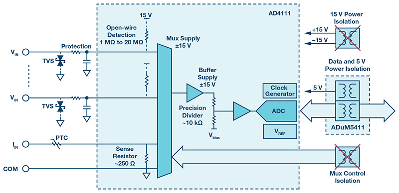
Typically, a limitation of single 5V designs is a lack of open wire detection, which is usually implemented using a high impedance resistor to the15V supply rail to pull an open connection to an out-of-range voltage. This is overcome by the AD4111, which boasts the unique capability of open-wire detection using a 5V or 3.3V supply. This separates open-wire detection from an out-of-range fault, further simplifying diagnostics. By including this feature internally on the AD4111, the need for a pull-up resistor on the front end is removed, and thus the need for the 15 V supply is also removed, as shown in Figure 2. Eliminating the ±15V supply reduces the complexity, area, and emissions of the isolation circuitry. For applications where open wire detection is not desired, an alternative generic, the AD4112, is available. This part has all the benefits of the AD4111 but without open wire detection.
System-Level Solution
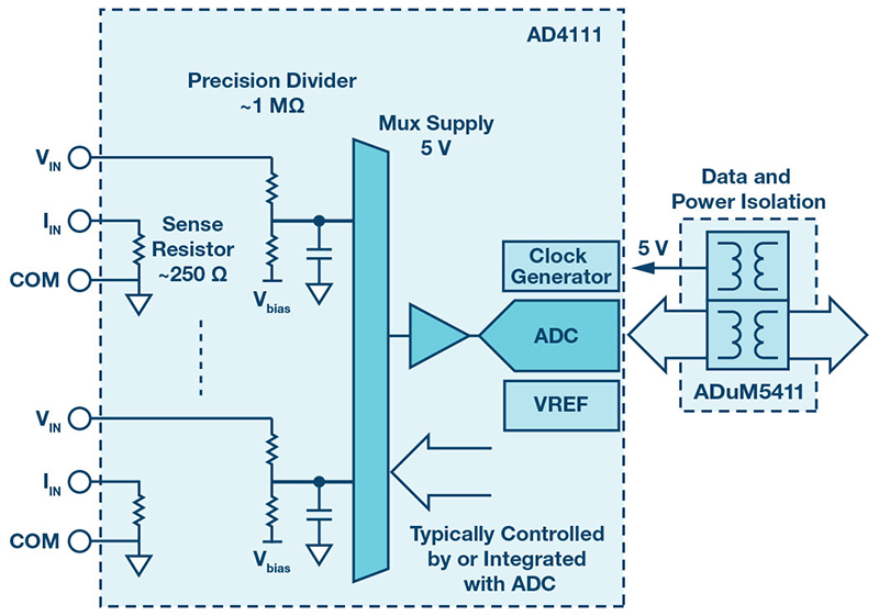
The AD4111’s integration of a voltage reference and internal clock help to reduce board size and BOM cost further, while allowing external components to be used if and when a higher precision and lower error conversion over temperature is required. Figure 2 and Figure 3 show typical high-end and low-end solutions, respectively. Highlighted in both Figure 2 and Figure 3 are the proportions of the signal chain that can be entirely replaced by the AD4111. The AD4111’s total unadjusted error (TUE) accuracy specifications were targeted to reach system level requirements. For many solutions, the accuracy may be sufficient to remove the need for any additional calibration. In existing high accuracy solutions, modules are often calibrated per channel. The AD4111 has been designed with highly matched inputs so that calibrating one input will provide a similar level of accuracy across all inputs.
Click image to enlarge
Figure 2. Typical high-end solution
Click image to enlarge
Figure 3. Typical low-end solution
EMC Testing
PLC and DCS modules often operate in harsh industrial environments and have to survive electromagnetic interference (EMI) conditions. This adds a greater level of complexity when designing an electromagnetic compatibility (EMC) capable input module since most devices are not rated for EMC, therefore designing the input protection and filtering circuitry becomes complex. This can add significant time to development in terms of design and testing. EMC labs are expensive to rent and failed testing can mean long delays until boards can be redesigned and retested. The AD4111 has been designed into a printed circuit board (PCB) that demonstrates a proven EMC solution. The board is characterized to ensure the circuit performance is not permanently affected by radiated radio frequency (RF) or conducted RF disturbances, and has been shown to have sufficient immunity against electrostatic discharge (ESD), electrical fast transient (EFT), and surge as per the IEC 61000-4-x set of standards. It has also been evaluated for CISPR11, where the radiated emissions for the board are well below the Class A limits. More information on the AD4111 EMC PCB can be found from AN-1572. This application note details all the necessary information on test procedures used, as well as board design schematics and layout to design an EMC proven input module for theAD41
Conclusion
The AD4111 is a system-level ADC with high levels of integration, which includes a comprehensive degree of configurability. Its ability to take ±10V voltage inputs and 0mA to 20mA current inputs, and operate from a single 5V or 3.3V supply with open-wire detection, along with its many otherfeatures, provides a unique solution for analog input module design. It comes in a 6mm × 6mm, 40-lead LFCSP and enables modules that once required a full complex PCB to now be replaced by a single device.