Smallest Dual-Channel Low-Side Gate Driver ICs
EiceDRIVER 2EDN dual-channel low-side gate driver ICs enable ultra-high-power density designs with small package size, while enhancing reliability and performance
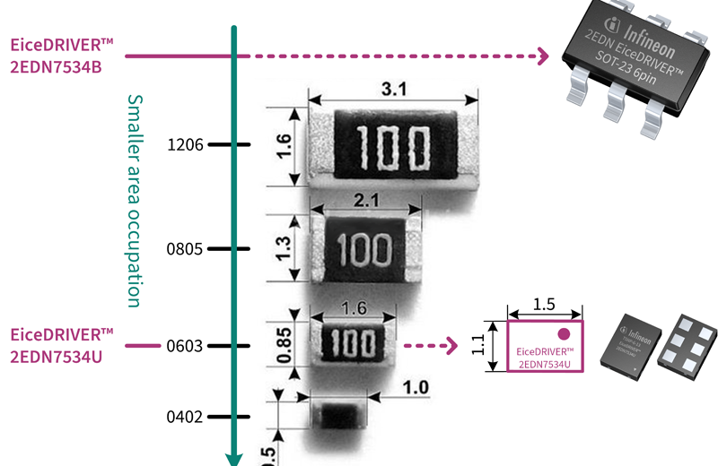
Figure 1: Footprint comparison: EiceDRIVER 2EDN7534U in TSNP vs SMD resistors
Overall power levels have been going up in Datacenter and Computing to supply the GPUs and CPUs used in emerging applications such as Artificial Intelligence, Computer Vision, and Machine Learning. Consequently, ever-increasing power density and efficiency requirements require innovation, not only on power switch technologies (e.g. GaN and SiC) and new topologies, but also demand advancements at the gate driver IC level. The operation of power semiconductors at hundreds of kHz or even MHz, combined with fast switching transients, pose new challenges for the gate driving circuit, that has to ensure safe and reliable operation in these critical infrastructure applications. Therefore, gate driver ICs play a key role in increasing the processed power while ensuring system protection and robustness. To support this, Infineon has recently introduced a new generation of dual-channel low-side gate driver ICs featuring 5 A source/sink output current capability, and the EiceDRIVER 2EDN family is now enlarged with products in a tiny leaded SOT23 (2.9 x 2.8 mm) and ultra-tiny leadless TSNP (1.5 x 1.1 mm) 6-pin packages. These new packages enable versatile placement, smaller footprint, and more optimized gate driving loops to improve switching performance in high-power density applications. Figure 1 puts into perspective the size of the new EiceDRIVER 2EDN7534U available in ultra-tiny TSNP package versus industry-standard SMD resistors, showing that it occupies a footprint area similar to a 0603 resistor.
Besides footprint options, the new EiceDRIVER 2EDN family offers an improved output stage with active clamping of the driving voltage, shorter undervoltage lockout (UVLO) startup time, and reduced current consumption. Furthermore, the high accuracy of propagation delay, allows the two outputs to be paralleled to double the current capability and also, to minimize dead-time losses in order to reach high system efficiency. Figure 2(right picture) shows an application example were having the two outputs in parallel is highly beneficial: the synchronous rectifier stage in hybrid switched capacitor converter (HSC) is typically operated without a gate resistor to achieve the fastest possible switching transients. Another application example for the EiceDRIVER 2EDNxx3x products is a typical center-tapped rectifier in Server SMPS as illustrated in Figure 2. The new EiceDRIVER 2EDN7534B in leaded SOT23 package offers the same performance as the other products in industry-standard leaded packages (DSO, TSSOP) but requiring a smaller PCB area, which is particularly important in space constrained designs.

Click image to enlarge
Figure 2a: CT rectifiers

Click image to enlarge
Figure 2b: SR in HSC topology
Figure 2a & 2b: Application examples for the new EiceDRIVER™ 2EDN7534 products
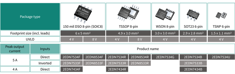
Product Family Overview
The EiceDRIVER 2EDNxx3x product family is available in five different packages: the three industry-standard packages 8-pin DSO (SOIC), TSSOP, and WSON, plus the tiny 6-pin SOT23 and TSNP designed for ultra-high power-density applications. For each package type there are different peak current capabilities, direct and inverted inputs, and dedicated undervoltage lockout levels to fit the target applications. A summary of the available products and features can be found in Table 1.
Click image to enlarge
Table 1: EiceDRIVER 2EDNxx3x product family overview table
Active Output Voltage Clamping
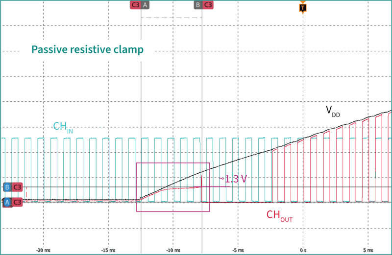
During start up, the driver bias voltage at the VDD pin has to ramp up, and the UVLO protection is intended to prevent the MOSFET from running in linear mode if a modulation scheme is applied to the gate driver IC. However, since in a generic gate driver IC the UVLO output clamping is usually implemented with a passive resistive clamp (Figure 3, left), the UVLO activation time is slow, and in some scenarios like microcontroller (MCU) and gate drivers supplied by different rails, this could result in several unwanted VGS pulses before the output is actively driven low.
Indeed, the activation time of a passive resistor-type clamp depends on the driver internal RC time constant, that is in the order of magnitude of several µs. During this long activation time the output is usually not properly clamped low and the MOSFET could be driven out of the triode region.

Click image to enlarge
Figure 3a: Generic passive RC-type clamp
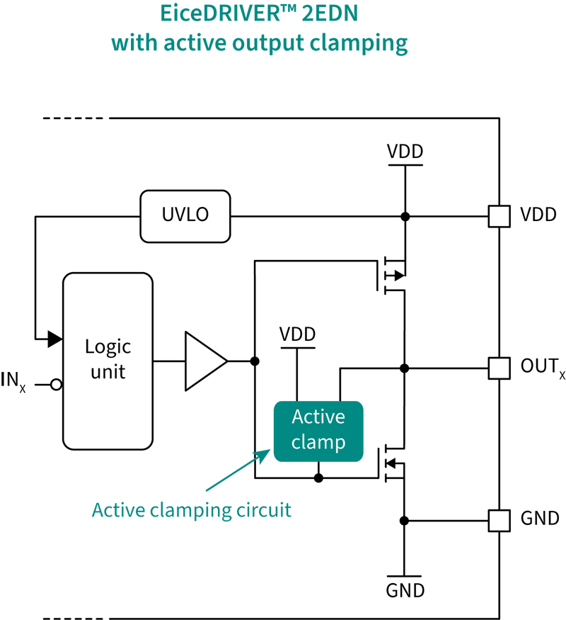
Click image to enlarge
Figure 3b: New generation of EiceDRIVER 2EDN
Figure 3a & 3b: Generic passive RC-type clamp (Top) vs active output voltage clamping mechanism in the new generation of EiceDRIVER 2EDN (Bottom)
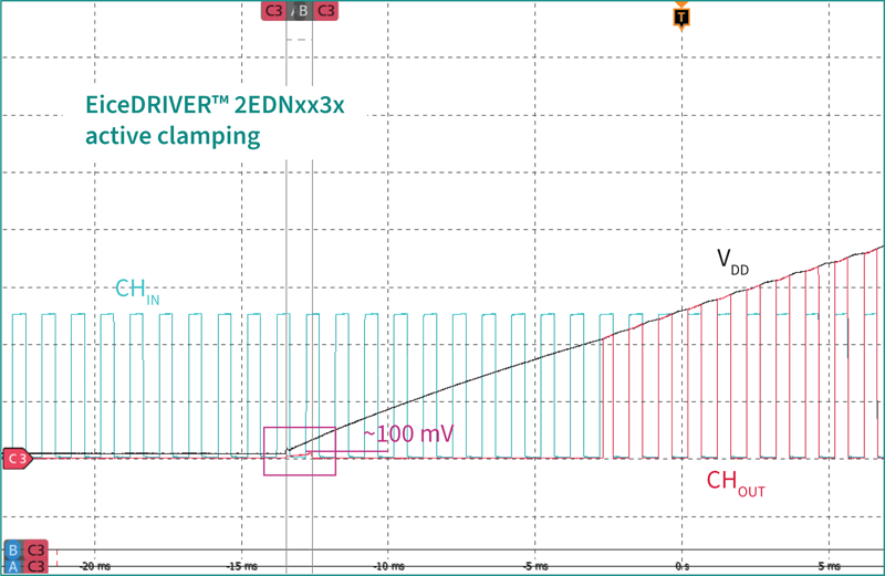
To overcome this issue, the output stage of the new EiceDRIVER 2EDN has been improved by introducing a fast and reliable active output voltage clamping mechanism as shown in Figure 3, right. The active clamping mechanism detects the voltage at the output pin and keeps the VGS in a safe-low condition until the UVLO is released. Consequently, the driver is then capable to react faster during start-up of the driver VDD voltage, preventing MOSFET switching when low VGS gate voltages are applied to the gate of the power switch.
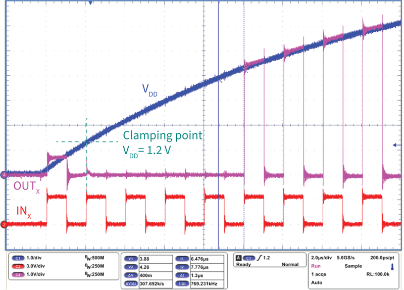
Figure 4 reports the behaviour of the EiceDRIVER 2EDN active output voltage clamping. As soon as the VDD voltage supply of the driver reaches 1.2 V, the active output voltage clamping mechanism is activated and the OUT pin is actively pulled-down to a safe-off level in an activation time of around 20 ns. The reaction is much faster than the RC time constant of passive clamp mechanisms that might take tens of microseconds or even more.

Click image to enlarge
Figure 4a: EiceDRIVER 2EDNxx3x active output voltage
Click image to enlarge
Figure 4b: EiceDRIVER 2EDNxx3x active output voltage
Figure 4a & 4b: EiceDRIVER 2EDNxx3x active output voltage clamping
Figure 5 compares the output waveforms of active output voltage clamping (EiceDRIVER2EDNxx3x) vs passive clamping present in similar parts available in the market in weak pull-up condition. The picture shows how the EiceDRIVER 2EDNxx3x behaves in a more reliable way, keeping the OUT voltage to a safe-low level during VDD start up.
Click image to enlarge
Figure 5a: Passive resistive clamp
Click image to enlarge
Figure 5b: EiceDRIVER 2EDNxx3x active clamping
Figure 5a & 5b: Passive vs active clamping in weak pull-up on OUT pin scenario
The active output voltage clamping mechanism is also preventing return-on of the MOSFETs that could occur from coupled voltage to the VGS due to displacement current flowing through the Miller capacitance Cgd during high dV/dt transients of the switching node. In this case, the output stage of the EiceDRIVER 2EDNxx3x detects the fast voltage transient, and quickly activates the active clamping mechanism to keep the gate to a safe OFF state when VDD is below the UVLO threshold. Figure 6 compares the two different clamping mechanisms.
Click image to enlarge
Figure 6a: Passive resistive clamp
Click image to enlarge
Figure 6b: EiceDRIVER 2EDNxx3x active clamping
Figure 6a & 6b: Passive vs active clamping in high dV/dt scenario
For all the considerations above, a fast and active output voltage clamping mechanism makes it possible to keep the OUTPUT pin at a safe-low condition in a short time, instead of having the gate of the switch exposed to unintended induced noise and potential unwanted linear mode operation.
Undervoltage Lockout Startup Time and Quiescent Current Consumption
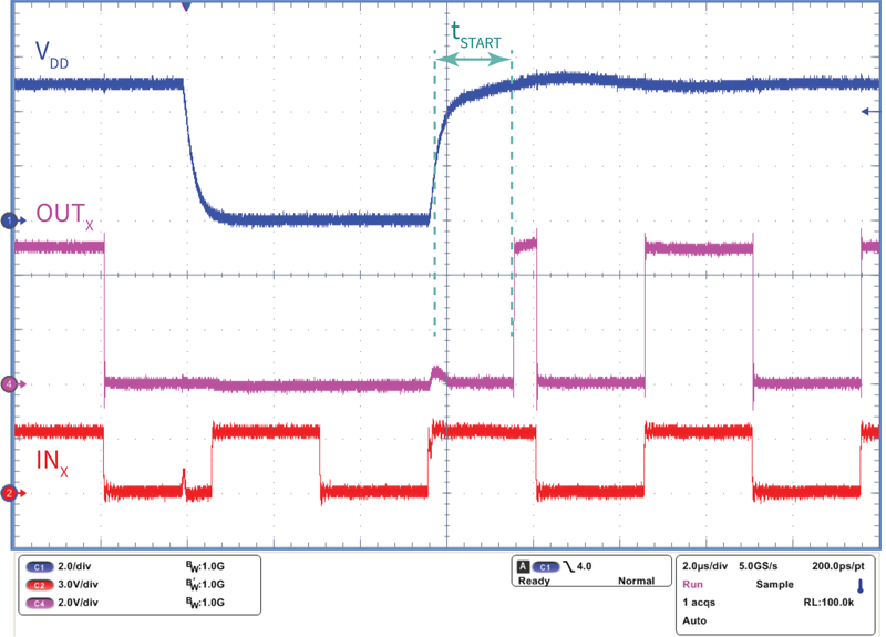
During system start-up, or when recovering from brown-out conditions, the time tSTART required by the driver to recover from the UVLO condition becomes critical. Indeed, if the system recovers from a UVLO condition and the MCU has a different supply than the gate driver IC, the MCU could send PWM pulses to the driver before UVLO is released. In this case, several pulses could be missed partially or totally until the driver supply voltage rises above the threshold (UVLOON).
Missing PWM pulses can lead to asymmetric on-time for the different positions of the switches, creating asymmetry in the circuit parameters and in the worst-case saturation of the magnetic components and unwanted surge currents. The longer the UVLO release time (tSTART), the higher the number of missed PWM pulses, the worse the asymmetry becomes. This is why it is so important that the active output voltage clamping mechanism reacts fast and accurately.
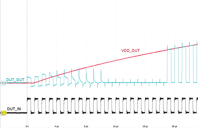
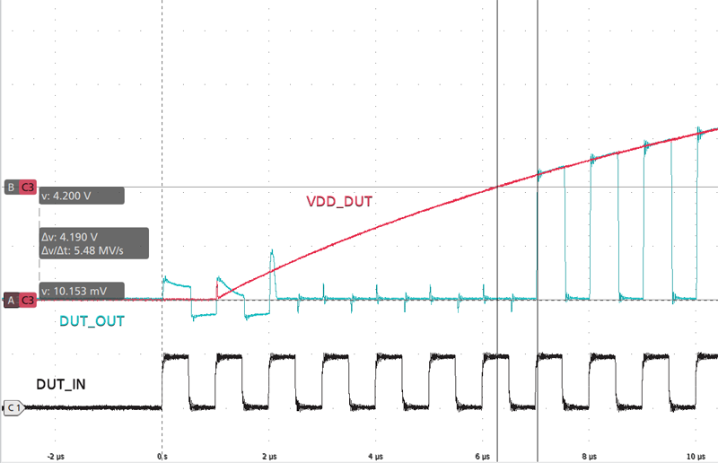
Most gate driver ICs available in the market have a UVLO startup time of 5 µs or longer. The new EiceDRIVER 2EDN gate driver ICs have a UVLO startup time (tSTART) of 1.8 µs (typical), leading to safe converter start-up and reliable operation by minimizing the number of PWM pulses when releasing UVLO. Figure 7 shows measured tSTART during UVLO recovery.

Click image to enlarge
Figure 7a: PWM input
Click image to enlarge
Figure 7b: PWM output
Figure 7a & 7b: PWM input and driver output during UVLO recovery of EiceDRIVER 2EDNxx3x
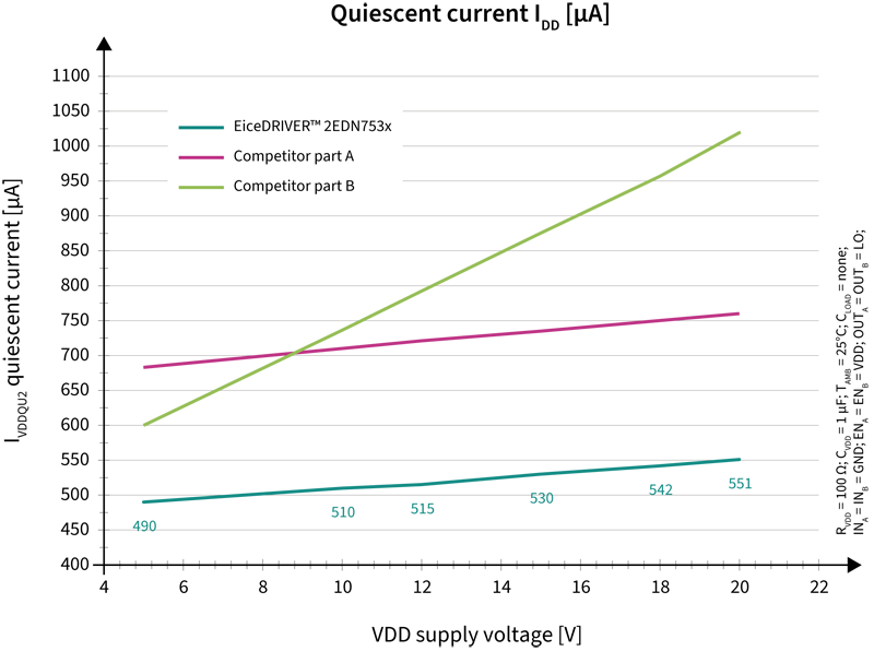
All the described improved features, and available in the new EiceDRIVER™ 2EDN family, are offered while maintaining low quiescent current compared to similar ICs available in the market, as shown in Figure 8. This helps to reduce the overall quiescent current consumption in standby conditions, in case the driver is enabled with no PWM signals applied.
Click image to enlarge
Figure 8: EiceDRIVER 2EDN quiescent current compared to products from other vendors
New Size Benchmark for Low-Side Dual-Channel Drivers
EiceDRIVER 2EDN is available in all the industry-standard 8-pin packages: DSO (SOIC), TSSOP, and leadless WSON. To enable a higher level of power density, Infineon introduced very compact 6-pins packages, the SOT23 and TSNP, by removing the two ENABLE pins that are not used (tied to VDD via internal pull-up) or simply shorted to VDD in some applications. The new SOT23 package allows us to save 73% of PCB layout area compared to its leaded DSO counterpart, and the TSNP package saves 81% space compared to the leadless WSON, as illustrated in Error: Reference source not found.

Click image to enlarge
Figure 9: Size comparison between new SOT23 and TSNP packages with industry-standard counterparts
This dramatic reduction in the overall size of the gate driver IC benefits layout placement, overall layout area especially in high power density applications, and allows optimal placement of the gate driver ICs to minimize gate driving loop. For instance, each EiceDRIVER™ 2EDN7534U, available in TSNP package, can be configured with paralleled channels and placed directly next to the gate pin of the OptiMOS™ to minimize the gate signal ringing, while doubling the maximum current capability due to accurate timing specifications.
Getting Benefit out of the New 2EDN’s Tiny Packages
The size reduction provided by the 2EDN gate driver IC packages make this device a good fit not only for driving low-side MOSFETs. Indeed, the two output stages could be reused to drive a high-frequency transformer and deliver hundreds of milliwatts of power, as required by most of the isolated bias supplies to supply the output stage of floating gate drivers.
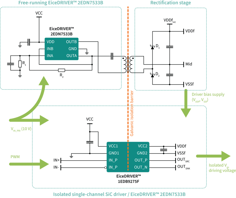
Figure 10 shows an example of circuital arrangement to generate two isolated positive and negative voltage rails by using EiceDRIVER 2EDN7533B in leaded SOT23 package. The two outputs OUTA and OUTB are configured as a full-bridge inverter and drive a compact high-frequency transformer (XT04) with low interwinding capacitance. The isolated gate driver IC and bias supply board (KIT_1EDB_AUX_SiC) sizes 8.5 mm x 17.5 mm only, making it suitable for placement in high-density high voltage power stages. It can provide up to 1.5 W average output power while keeping very good load regulation. Different output positive and negative voltage rails can be obtained to match different SiC MOSFETs. By properly trimming the circuit, +18V/-1V, +18V/-5V, +15V/-4V and +20V/-3V are possible from a 10 V input unipolar supply rail. Same approach can be followed using EiceDRIVER 1EDN for GaN HEMT devices as demonstrated in KIT_1EDB_AUX_GaN. The board also includes an optional circuit to achieve 1% voltage regulation using a TL432 shunt regulator.
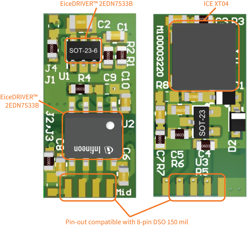
The cross-section of KIT_1EDB_AUX_SiC board (Figure 11) is designed to be soldered on the footprint of a DSO-8 single channel isolated gate driver IC (e.g. EiceDRIVER 1EDB6275F), and used as in a daughter-card approach in place of an existing DSO8 driver without isolated supply.
Click image to enlarge
Figure 10: Isolated gate driver IC with a configurable floating bipolar bias supply for SiC MOSFETs (KIT_1EDB_AUX_SiC)
Click image to enlarge
Figure 11: KIT_1EDB_AUX_SiC, compatible with EiceDRIVER 1EDBxxxxF footprint
Summary
In summary, this article covers the advantages and improved features of the Infineon EiceDRIVER 2EDNxx3x dual-channel low-side gate driver ICs. The innovative features include fast active output voltage clamping and shorter undervoltage lockout start-up time, which improve overall system robustness and reliability.
Above all, the new generation of EiceDRIVER 2EDN products sets a new benchmark in terms of available package size in the market by introducing two new 6-pin packages: leaded SOT23 and leadless TSNP. These new packages enable innovative 48 V DC-DC intermediate bus converter (IBC) topologies to achieve ultra-high power density designs in high performance computing systems, without compromising the high performance of the standard 2EDN products.
Overall, EiceDRIVER 2EDN products matched with Infineon’s MOSFETs, can push high power applications to new levels of power density, maintaining the flexibility of design and the scalability of a discrete solution with separated gate driver and switch.


.jpg)
