The race to design high-efficiency, high-power-density inverters
Due to the ever-increasing demand for a clean and renewable source of energy, installing solar systems has accelerated significantly in the last decade. Contemporary solar applications require very highly efficient, power-dense and lightweight grid-tied inverters.
Traditionally, IGBT has been the device of choice in both three-phase and single-phase (≤10 kW) solar inverter designs while superjunction (SJ) MOSFETs (600/650 V) also have been used in some single-phase designs. But both IGBTs and SJ MOSFETs have their drawbacks that limit the efficiency and power density of inverters.
Recently engineers have focused on two different approaches to improve efficiency and power density of single-phase inverters to even higher levels. One is replacing IGBT and SJ MOSFETs with wide bandgap devices like SiC MOSFETs. Another approach is replacing the traditional topologies (H4, H5, H6, etc.) with multilevel topologies using lower voltage silicon MOSFETs.
As we discuss in this article, using these two approaches efficiency up to 99% and very high power density inverters can be designed.
Replacing IGBTs and SJ MOSFETs with SiC MOSFETs
IGBTs suffer from high switching losses that limit their use to only frequencies less than 20 kHz. On the other hand, high Qrr, slow body diode and relatively high RDS(on), limit SJ MOSFETs usage in inverter applications. These constraints limit the efficiency and power density of conventional single-phase solar inverters to around 98% and below.
On the contrary, SiC MOSFETs offer very fast parallel diode ,very low Qrr and switching losses much lower than IGBTs. Recently, Infineon has introduced its 650 V silicon carbide CoolSiC™ MOSFET that can directly replace IGBTs and SJ MOSFETs with no need for change in the inverter topology. SiC MOSFETs enable switching at a higher frequency which means a significant reduction in magnetic size, capacitor filter, and enclosure size. As the power level goes up, reduction in size and weight will save costs.
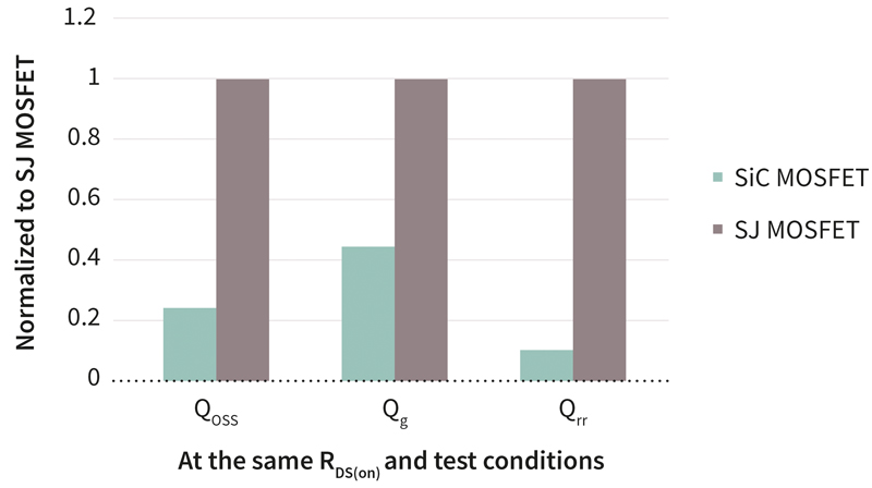
Figure 1 clearly indicates how by replacing a SJ with a SiC MOSFET, switching loss decreases significantly. As shown in figure 1, considered in terms of drain-source charge (Qoss), recovery charge (Qrr) and gate charge (Qg), SiC MOSFETs (i.e., the CoolSiCTM MOSFET 650 V) have superior figures-of-merit than the best alternative SJ MOSFETs (i.e., 600 V CoolMOSTM CFD7).
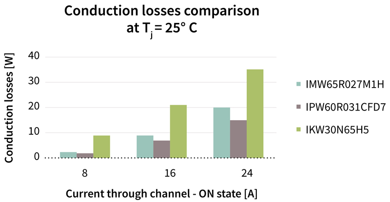
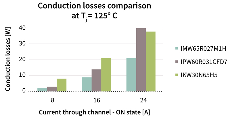
Figure 2a shows the conduction loss comparison of three best in class devices including IGBT IKW30N65H5 (650 V), SJ MOSFET IPW60R031CFD7 (600 V) and SiC MOSFET IMW65R027M1H (650 V) at a junction temperature of 25°C. Figure 2b displays how conduction losses change over varying currents at 125°C. Firstly, as can be seen, the conduction losses of IGBTs are significantly higher than of the other devices at 25 °C, however, it doesn't rise significantly as temperature increases to 125 °C. Secondly, also shown in the graph that the conduction loss of the SJ MOSFET at 125°C is two times higher than at 25°C for the same device. Thirdly, looking at the data of the SiC MOSFET, it shows only approximately 20 percent conduction loss increase over this temperature range. This makes a clear difference between Si and SiC MOSFET technologies, especially at high current, high-temperature operating conditions.
Click image to enlarge
Figure 2a: Conduction losses over varying currents at 125°C
Click image to enlarge
Figure 2b: Conduction losses change over varying currents at 125°C
Replacing traditional topologies with multilevel topologies
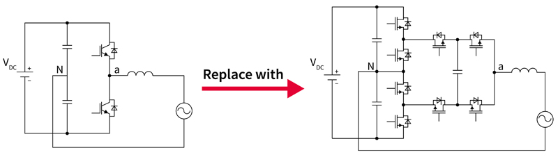
Traditionally topologies like H4, H5, H6, and so on using IGBTs and SJ MOSFETs have been widely used in single-phase solar inverter applications. One novel approach that has gained more attention recently to improve efficiency and power density is to replace these conventional topologies with multilevel topology (for an example see Figure 3) based on medium-voltage MOSFETs (60 V to 300 V). Infineon's OptiMOS™ 5 product family of medium-voltage MOSFETs have excellent figures-of-merit (extremely low RDS(on) x Qg, RDS(on) x Qrr, and RDS(on) x Qoss) and enable very high-efficiency (up to 99 percent) and power-density designs, when used in multilevel inverters.
Click image to enlarge
Figure 3: Increase efficiency and power density by replacing conventional topologies with multilevel topology
Compared to the conventional design, the inductor and capacitor filter size is multiple times smaller in a multilevel inverter. This, along with the need for a smaller cooling system, allows for a much lighter design with a smaller enclosure. On the other hand, due to the lower voltage rating of MV MOSFETs, more MOSFETs are used in a multilevel design compared to conventional topologies. This also means that the generated heat due to the power loss in the multilevel inverter (which is less than in a conventional design) is distributed among more devices. As a result, the thermal management of the multilevel inverter is more efficient which paves the way for heatsink-free and fanless designs.
In a typical single-phase string inverter (power ≥ 3 kW), semiconductors commonly account for less than 10 percent of the overall costs. However, cooling systems and magnetics are usually more expensive. While semiconductor device prices are continuously dropping, the cost of other components such as magnetic and heatsinks remain unchanged. That means for single-phase solar inverters with a full power capability of more than 3 kW, where the cost of mechanical components is a significant portion of the design, using multilevel inverter contributes to production cost saving.
One other big advantage of multilevel inverter is that lower loss per MOSFET allows using SMD packages. Utilizing SMD packages helps with assembly cost saving by applying automated pick and place process. In addition, the reduced package inductances improve the switching performance at higher frequencies.
Scalability is another big advantage of multilevel inverters. A multilevel inverter can be easily scaled to higher power design with almost the same design and PCB layout.
But to mention, multilevel inverters face one big challenge too. Compared to conventional topologies, there is a need for a greater number of gate drivers and isolated power supplies to power them up. This challenge is tackled by using very cost-effective, low-power multi-output flyback power supplies (≤ 1 W).
A 4 kW heatsink-free, fanless, medium-voltage MOSFET-based multilevel inverter
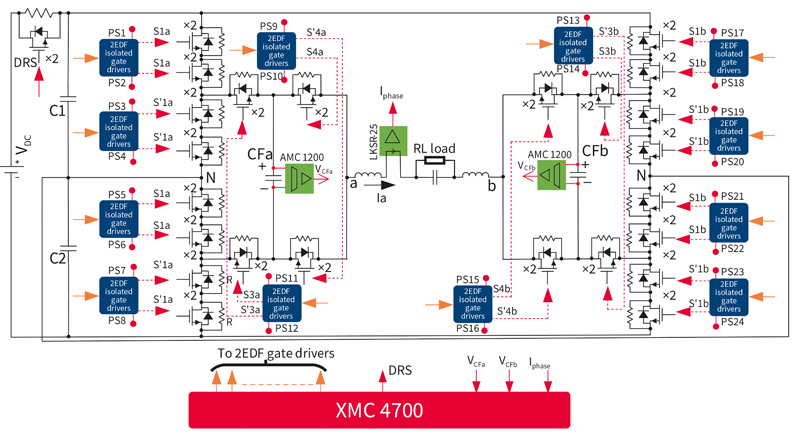
In this section, a 4 kW, five-level single-phase flying-capacitor-based active neutral point clamped multilevel inverter demonstration board will be introduced. This fanless, heatsink-free design offers more than 99 percent peak efficiency and full power efficiency as of 98.7 percent.
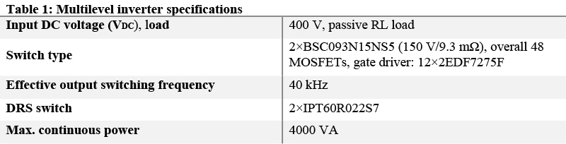
Figure 4 shows the schematic of the multilevel inverter demonstration board while Table 1 lists the specification of this inverter. Given that this is a five-level inverter, 150 V BSC093N15NS5 (9.3 mΩ, OptiMOS™ 5) MOSFETs were used despite the 400 VDC_bus voltage. This device has much better figures-of-merit(orders of magnitude) compared to IGBTs and SJ MOSFETs.
Click image to enlarge
Figure 4: Schematic of the multilevel inverter demonstration board
Click image to enlarge
Table 1: Inverter specifications
Figure 5 shows the efficiency of the demonstration board in relation to the output power. The maximum efficiency (approximately 99.1 percent) is achieved at around 2 kW. At full load (4 kW), the efficiency is still very high, at around 98.7 percent which explains why this multilevel inverter can work continuously without the need for any heatsink or fan.

Click image to enlarge
Figure 5: Efficiency of the demonstration board in relation to the output power
Conclusion
Now the question for an inverter designer who is looking for higher efficiency and power density is which one of the above-described solutions to choose. Replacing IGBTs and SJ MOSFETs with SiC MOSFETs or replacing the conventional with the multilevel topology?
Beyond question, replacing silicon-based devices with SiC MOSFETs requires less effort compared to altering the topology. But although this change to SiC will increase efficiency and power density, still not as much as the multilevel solution. A heatsink is still needed and for a higher power range (> 5 kW), forced cooling probably should be also considered.
Even though the multilevel topology is more complex than conventional topologies, if a designer has previous experience with this type of topology or willing to learn and invest R&D effort into it, moving to the multilevel inverter is recommended as 99 percent of efficiency and very high power density can be easily achieved.
 Single.jpeg)