
Boosted by advanced digital isolation technologies
Figure 1: Single-Stage, Single-Phase Inverter Block Diagram
The modern power grid will feature photovoltaic (PV) power systems that offer a sustainable alternative to fossil-fueled power plants. PV power systems consist of multiple components such as PV panels that convert sunlight into electricity modules, mechanical and electrical connections and mountings, and solar power inverters, which are essential to conveying solar-generated electricity to the grid. PV panels convert sunlight into dc voltage, which must be converted to high-voltage ac to minimize line losses and enable longer power transmission distances. The PV solar inverter performs this dc to ac conversion and is the most critical component in any PV power generating system. However, this is just one key function that the PV inverter provides. The PV inverter also offers a grid disconnect capability to prevent the PV system from powering a disconnected utility; that is, an inverter remaining on-line during grid disconnect, or delivering power through an unreliable connection can cause the PV system to back-feed local utility transformers, creating thousands of volts at the utility pole and endangering utility workers. Safety standard specifications IEEE 1547 and UL 1741 state that all grid-tied inverters must disconnect when ac line voltage or frequency is not within specified limits, or shut down if the grid is no longer present. Upon reconnect, the inverter cannot deliver power until the inverter detects rated utility voltage and frequency over a five minute period. But again, this is not the end of the inverter's duties. The inverter also compensates for environmental conditions that affect power output. For example, PV panel output voltage and current are highly susceptible to variations in temperature and light intensity per cell unit area (referred to as "irradiance"). The cell output voltage is inversely proportional to cell temperature, and cell current is directly proportional to irradiance. The wide variation of these and other key parameters causes the optimum inverter voltage/current operating point to move about significantly. The inverter addresses this issue by using closed-loop control to maintain operation at the so-called maximum power point (MPP), where the product of voltage and current is at its highest value. In addition to these tasks, the inverter also supports manual and automatic input/output disconnect for service operations, EMI/RFI conducted and radiated suppression, ground fault interruption, PC-compatible communication interface and more. Encased in a ruggedized package, the inverter is capable of remaining in full-power outdoor operation for more than 25 years. No small feat! Taking a Closer Look The single-phase PV inverter example shown in Figure 1 uses a digital power controller and a pair of high-side/low-side gate drivers to drive a pulse width modulated (PWM) full-bridge converter. Full bridge topology is typically used in inverter applications because it has the highest power carrying capability of any switch mode topology. Referring to Figure 1A, the PWM voltage switching action synthesizes a discrete (albeit noisy) 60 Hz current waveform at the full bridge output. The high-frequency noise components are inductively filtered and produce the moderately low amplitude 60 Hz sine wave shown in Figure 1B. The filtered waveform is then passed through an output transformer that performs three functions: 1) it further smoothes the ac waveform; 2) corrects the voltage amplitude to meet specified grid requirements; and 3) galvanically isolates the inverter's dc input from the high-voltage ac grid. PV inverter design is chock-full of design trade-offs that can cause the designer to lose much hair or stomach lining if the wrong trade-offs are made. As an example, PV systems are expected to operate reliably and at full rated output for a minimum of 25 years, and yet they need to be competitively priced, forcing the designer to make tough cost/reliability trade-offs. PV systems need highly efficient inverters because, after all, higher efficiency inverters run cooler and last longer than their lower efficiency counterparts, and they generate cash savings for both the PV system manufacturer and user. The "brains" behind the inverter is its controller, usually a digital power controller (DPC) or digital signal processor (DSP). Typically, the controller's firmware is implemented in a state machine format for the most efficient execution using non-blocking (fall-through) code, which prevents execution from inadvertently entering an endless loop. Firmware execution is hierarchal, typically servicing the highest priority functions more frequently than lower order functions. In the PV inverter case, isolated feedback loop compensation and power switch modulation are usually the highest priorities, followed by critical protection functions to support UL 1741 and IEEE 1547 safety standards, and then followed by efficiency control (MPP). The remaining firmware tasks pertain mostly to optimizing operation at the present operating point, monitoring system operation and supporting system communication. The PV inverter's exposure to blazing heat and/or freezing cold temperatures for 25 years causes one to take pause when considering the components used in the inverter's innards. Clearly, components such as electrolytic capacitors that filter-out ripple and optocouplers that provide galvanic isolation have no chance of "going the distance." Electrolytic capacitors dry out and drop dead, and the optocoupler's LED brightness gradually fades to a dim glow, halting operation. Workarounds for these delicate components consist of replacing electrolytic capacitors with high-value film capacitors (higher reliability, but obviously higher cost).The optimal long-term solution is to dismiss the optocoupler in favor of modern CMOS isolation components. CMOS process technology offers the advantages of high reliability, cost effectiveness, high-speed operation, small feature size, low operating power and operating stability over voltage and temperature extremes, and many other desirable attributes. And unlike the Gallium Arsenide (GaAs) process technology used in optocouplers, devices fabricated in CMOS have no intrinsic wear-out mechanisms. The underlying CMOS isolation cell is capacitive, fully differential and highly optimized for tight timing performance, low power operation, and high immunity to data errors caused by external fields and fast common mode transients. In fact, the advantages brought by CMOS process technology combined with proprietary silicon product design make possible robust, "near ideal" isolation devices unlike the world has ever seen. These devices offer across-the-board greater functional integration, substantially higher reliability (60+ year isolation barrier lifetime); 40°C to +125°C continuous operation at maximum VDD, and substantial gains in performance, power consumption, board space savings and ease-of-use.
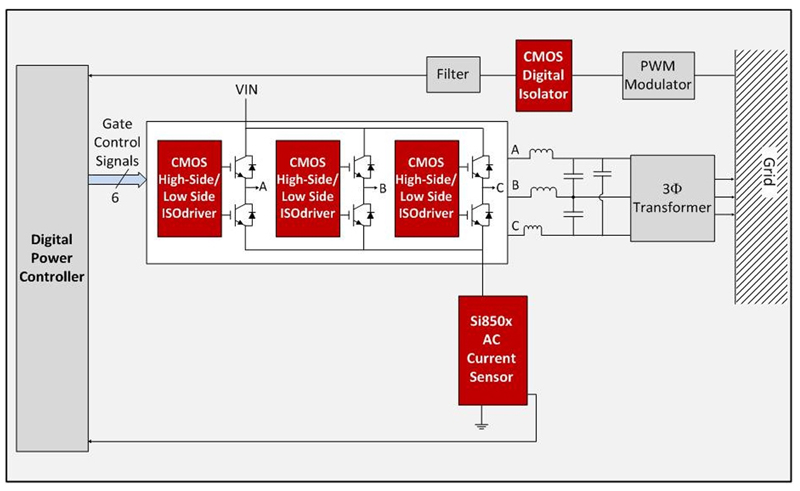
21st Century Component Solutions for PV Inverters PV inverter architecture does not end with the single-phase, transformer-based inverter shown in Figure 1. Other common types include high-frequency, bipolar, 3-phase, transformerless and battery-powered inverters. While these topologies differ from one another, they often share the need for the same component solutions. The block diagram in Figure 2 shows several CMOS isolation devices used in a transformer-based, three-phase inverter. This is a classic closed loop architecture where the digital controller modulates the power switch duty cycle to force the PV system output voltage amplitude and phase to exactly match that of the grid. These isolated gate drivers integrate safety certified galvanic isolation (rated at 1kV, 2.5kV or 5kV) and high-side level shifting functions in a single package, eliminating the need for external isolation devices. Each driver output is isolated from the other, enabling a mix of negative and positive voltage rail voltages to be used without latch-up. Current feedback to the controller is provided by a single 4 mm x 4 mm x 1 mm CMOS isolated ac current sensor (its 1kV isolation rating is limited by package size - larger packaged versions are rated up to 5kVrms). These monolithic sensors have a wider temperature range, higher accuracy and higher reliability compared to current sense transformers. The sensor is reset on a cycle-by-cycle basis using the inverter gate control signals generated by digital controller, eliminating the need for external reset circuitry. The grid feedback is a critical part of the system feedback control mechanism. A resistive attenuator is used to reduce the grid voltage to a range that is compatible with the PWM modulator, which converts the sine wave input to a discrete PWM waveform and safety isolated by the CMOS digital isolator. Going Forward As PV inverters expand in functionality, designers will demand more integrated, application-specific component-level devices that will further leverage and drive innovation in CMOS isolation. As these events unfold, PV power systems will become more widespread and ultimately a viable member of the utility mainstream that will significantly reduce our dependence on fossil fuels. www.silabs.com


