Solved Problems Look Easy - USB-PD Solutions: Part 1 of 4
USB-PD solutions from Infineon
Avoid complexity, incompatibility and shorten time-to-market! Infineon with its broad portfolio of high-performing and high-quality USB-PD solutions help engineers break through the barriers in fast charging designs at a competitive cost
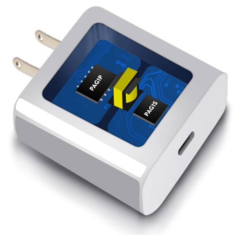
Nowadays, people have many rechargeable battery-powered mobile devices – smartphones, tablets, wireless headphones, and laptops are all in one bag. But carrying all or some of these around together with their respective chargers and cables, that is usually a mess... But what if there is a solution to reduce the number of chargers and cables to a single one which can not only charge your devices but can do it faster than before? Fortunately, it is made possible by the USB-PD (power delivery) which is a charging technology suitable for all devices.
From a technology point of view, the latest trends push the envelope of form factors, charging power, battery capacity, and charging time. Translating these needs into performance requirements means an increase in power density and efficiency. These are the drivers in the charger market today and there are several ways – various combinations of topologies and power technologies - to meet the expectations.
Solutions of choice for fast chargers
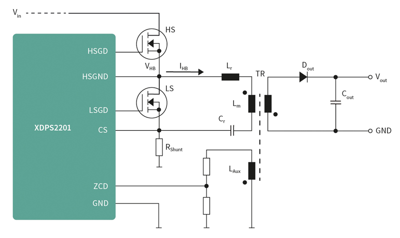
Let’s first look at the topology. Flyback seems to be the most widely used in charger designs due to its lower cost and ease of design compared to other topologies. However, as in a traditional flyback converter the transformer is usedforenergy storage, it results in a larger transformer. This limits the maximum achievablepower density. To overcome this limitation coming from the transformer size,the solution is to increasethe switching frequency.But as the frequency increases,the energy losses in the parasiticelements (mainly transformer leakage inductance) and MOSFET capacitance become more significant. To resolvethe issues caused by thehigherswitching frequencies, different variants of the soft-switching flyback topology have become popular, such as the digital forced-frequency-resonant (FFR) enabled by the XDPS21071 and XDPS21081 digital controllers from Infineon's portfolio.
In recent years, new technologies such as GaN-based devices together with soft-switching flybacks seemed to be able to achieve higher switching frequencies solving the two main limitations of high-power-density adapters: recycling energy from the parasitic components while reducing the size of the transformer. Nevertheless, the higher switching frequencies are not exempt from problems. Faster switching frequencies raise new EMI challenges. Another limitation of this solution is the higher cost of the “special” devices – GaN power switch and ZVS controller - in a market where the total system cost is very sensitive.
A new creatively titled asymmetrical duty-cycle flyback converter is a hybrid between a flyback and a forward converter. It addresses the main problems related to high-density adapters operating at moderate switching frequencies. It can ensure zero voltage switching (ZVS) and zero current switching (ZCS) over line and load, thus enabling higher efficiency.
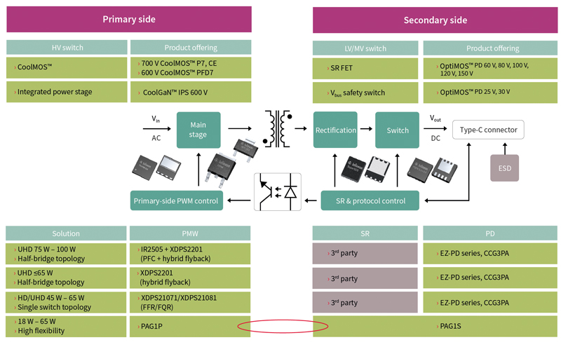
To ensure that design engineers are able to meet their design targets, Infineon offers a broad range of solutions with a comprehensive semiconductor portfolio of high- and low-voltage power MOSFETs, USB-PD protocols as well as digital soft-switching controllers that provide excellent power density (see Figure 1):
How to choose the right controller?
The charger market is typically end-consumer-orientated and as such is quite cost-sensitive and focuses on high performance. For a design going beyond 91 percent efficiency, the two-chip PAG1 solution is highly recommended due to its excellent price-performance characteristic. The solution comprises of a primary start-up controller PAG1P, and a single-chip secondary-side controller PAG1S which integrates synchronous rectification control and USB-PD protocol control. In particular, the PAG1S is a programmable device offering great flexibility, allowing users to fine-tune the QR valley value at which the converter switches across line/load voltages. It makes it possible to optimize the system efficiency without changing the external hardware components.
In order to obtain better performance (e.g., 92 percent), the digital-based XDPS21081 ZVS controller is the most suitable. This is the industry’s first flyback controller with ZVS on the primary side to achieve high efficiency with simplified circuitry and economical switches, thereby reducing BOM cost. By negative magnetization, the FFR switching scheme can reduce the losses associated with today’s valley-switching type controllers without sacrificing the design simplicity of the fixed-frequency switching schemes. Besides, the digital controller can adjust many parameters to simplify the BOM. It also provides great flexibility, allowing engineers to tailor-make their designs according to different system specifications.
If even higher efficiency (e.g., 93 percent) is required, an asymmetric flyback topology is recommended. At Infineon, this topology is called hybrid flyback because the converter operates in mixed flyback/forward mode. The hybrid topology lays the foundation for the highest conversion efficiency by using the magnetization current to achieve ZVS on the primary-side half-bridge and ZCS on the synchronous rectification switch.
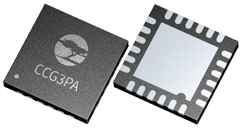
When the main design requirement is the firm compatibility with the USB-C protocol,the highly integrated USB Type-C port controller EZ-PD™ CCG3PA is recommended. The CCG3PA complies with the latest USB Type-C and PD standards and is targeted for PC power adapters, mobile chargers, car chargers, and power bank applications. In such applications, the CCG3PA provides additional functionalities and BOM integration advantages. The CCG3PA uses proprietary M0S8 technology from Cypress (the company is part of Infineon Technologies) with a 32-bit Arm® Cortex®-M0 processor, 64-KB flash, a complete Type-C USB-PD transceiver, all termination resistors required for a Type-C port, an integrated feedback control circuitry for voltage (VBUS) regulation, and system-level ESD protection. It is available in 24-pin QFN and 16-pin SOIC packages.
Click image to enlarge
Figure 2: The highly integrated USB Type-C port controller EZ-PD™ CCG3PA in 24-pin QFN
How to choose the right power switch?
Infineon is the leader in power discrete devices, providing many high-performance power switches that help improve power management efficiency. Just recently, Infineon has released a complete product portfolio tailored to meet the latest charger design requirements at an affordable cost.
The new 600 V CoolMOS™ PFD7 series and the 700/800 V CoolMOS™ P7 series offer cost-competitiveness with improved technology that reduces switching- and conduction losses. Also, an integrated gate-source Zener diode is featured for improved ESD protection and system reliability during operation.
By having a lower total gate charge (Qg) as well as lower energy storage in the MOSFET output capacitance (which needs to be burned off every cycle during hard switching (Eoss)), the switching losses of the MOSFETs are improved. By reducing these total charges, which are dissipated in each switching cycle, the efficiency of the system at light loads can be improved.
Improved technology can reduce the conduction losses of the device, thereby improving the temperature coefficient of the device. The RDS(on) of a MOSFET is typically rated at 25°C, but during operation, the junction temperature will be higher. Compared with the previous-generation C6 technology, the PFD7/P7 series offers a 10 percent reduction in RDS(on) at 100°C, thereby reducing the conduction losses. Although the common industry standard is that the RDS(on) is 2x the datasheet value at 125°C, now with this latest technology it is reduced to 1.9x only.
With these improvements in conduction losses and switching losses, the new technology provides the possibility to shift to higher RDS(on) MOSFETs to reduce overall system costs or to increase overall system switching frequency to reduce the form factor and the cost of passive component.
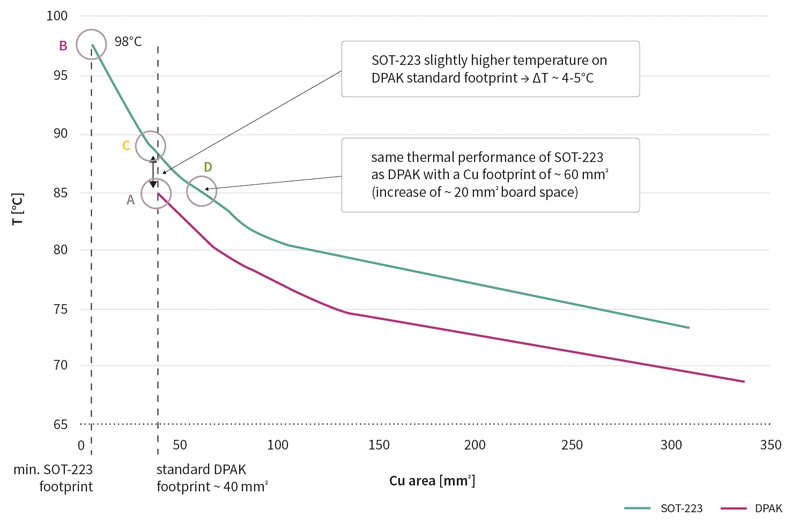
Right-fit package selection helps to improve the performance of the USB-PD charger soluion. Let’s take the cost-effective SOT-223 package as an example. It’s the perfect drop-in replacement for DPAK at a lower cost. Figure 3 shows that the SOT-223 package can achieve thermal performance similar to DPAK.
Click image to enlarge
Figure 3: Thermal simulation of junction temperature at 250 mW and an ambient temperature of 55°C
The ThinPAK package is characterized by very low source inductance, a separate driver source connection for clean gate signals, and a highly improved commutation loop (MOSFET, diode, cap) to achieve the lowest stray inductance, which helps to reduce VDS overshoots. As a result, the ThinPAK package enables faster and more efficient switching of power MOSFETs, and is also easier to handle in terms of switching behavior and EMI.
Click image to enlarge
Figure 4: ThinPAK’s improved commutation loop reduces stray inductances hence VDS overshoots as well
For the secondary side, Infineon has released a tailor-made OptiMOS™ PD series for synchronous rectification and loading switching of USB-PD chargers. The family features MOSFETs offering low on-state resistance (RDS(on)), lower switching losses as well as low gate-, output- and reverse recovery charges. This reduction in overall losses results in an excellent price/performance ratio, which helps to reduce the overall system BOM cost. The availability of logic-level variants allows these parts to be fully driven from 4.5 V or directly from microcontrollers, thereby reducing the part count in the application. In addition, the PQFN 3.3 x 3.3 and SuperSO8 packages can shrink the size of USB-PD chargers.
The latest reference design
Infineon recently released the ready-to-use 65 W 20 W/in3 (50 CC) USB-PD digital FQR XDPS21081 reference design (Figure 5). This silicon-based solution offers robustness, high power density, low cost, and productive design. Commodity components are used to reduce production complexity.

Click image to enlarge
Figure 5: Infineon’s high-density 65 W reference design for high performance with ease-of-use at an affordable cost
In a nutshell
The USB-PD protocol is unifying the charger market. Infineon offers a comprehensive portfolio to enable high-density USB-PD charger designs at a competitive cost. A large variety of power MOSFETs, controllers, reference designs are available to help design engineers to find the best fit for their design requirements. The digital-based XDP™ controller, the XDPS21081 brings a new control method for ZVS/ZCS operation to enhance flyback converters; the tailor-made superjunction high-voltage CoolMOS™ and low-voltage OptiMOS™ families provide cost-effective solutions for power switches to improve market competitiveness; the extensive product portfolio of USB-C protocol controllers can improve wired communication capabilities. With the flexibly variable reference designs, design engineers can easily develop the right-fit USB-PD charger solution.
Discover our reference designs, boards and design support documents at www.infineon.com/usb-pd!