Stress-Free Metallic Films Pave the way for Next-Gen Circuitry
Optimized sputtering technique helps minimize stress in tungsten thin films
Researchers from Tokyo Metropolitan University have used high power impulse magnetron scattering (HiPIMS) to create thin films of tungsten with unprecedentedly low levels of film stress. By optimizing the timing of a "substrate bias pulse" with microsecond precision, they minimized impurities and defects to form crystalline films with stresses as low as 0.03 GPa, similar to those achieved through annealing. Their work promises efficient pathways for creating metallic films for the electronics industry.
Modern electronics relies on the intricate, nanoscale deposition of thin metallic films onto surfaces. This is easier said than done; unless done right, "film stresses" arising from the microscopic internal structure of the film can cause buckling and curving over time. Getting rid of these stresses usually requires heating or "annealing". Unfortunately, many of the best metals for the job e.g. tungsten have high melting points, meaning that the film needs to be heated to over 1000 degrees Celsius. Not only is this energy intensive, but it severely limits which substrate materials can be used. The race is on to create films out of high melting point metals without these stresses in the first place.
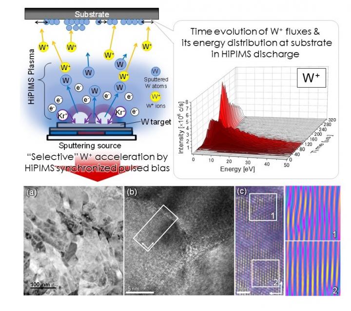
A team led by Associate Professor Tetsuhide Shimizu of Tokyo Metropolitan University have been working with a technique known as high power impulse magnetron scattering (HiPIMS), a sputtering technique. Sputtering involves applying a high voltage across a metallic "target" and a substrate, creating a plasma of charged gas atoms which bombards the metallic target and forms a charged metal vapor; these metal ions fly towards the substrate where they form a film. In the case of HiPIMS, the voltage is pulsed in short, powerful bursts. After each pulse, it is known that there is some separation between the arrival of metal and gas ions at the substrate; a synchronized "substrate bias" pulse can help selectively accelerate the metal ions, creating denser films. Yet despite many efforts, the issue of residual stress remained.
Now, using argon gas and a tungsten target, the team looked at how ions with different energies arrived at the substrate over time in unprecedented detail. Instead of using a bias pulse set off at the same time as the HiPIMS pulse, they used their knowledge of when different ions arrived and introduced a tiny delay, 60 microseconds, to precisely select for the arrival of high energy metal ions. They found that this minimized the amount of gas ending up in the film and efficiently delivered high levels of kinetic energy. The result was a dense crystalline film with large grains and low film stress. By making the bias stronger, the films became more and more stress-free. The efficient delivery of energy to the film meant that they had, in fact, achieved a similar effect to annealing while they deposited the film. By further swapping out argon for krypton, the team realized films with a stress as low as 0.03 GPa, comparable to what can be made with post-annealing.
An efficient pathway to stress-free films will have a significant impact on metallization processes and the manufacture of next-generation circuitry. The technology may be applied to other metals and promises big gains for the electronics industry.
EurekAlert!, the online, global news service operated by AAAS, the science society: https://www.eurekalert.org/pub_releases/2021-07/tmu-spt063021.php