Switched Capacitor Converter for Energy Transfer, Conversion
Switched capacitor converters offer a simple, inductor-free alternative to buck or boost converters
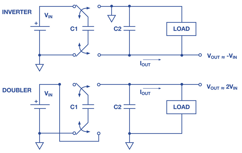
Figure 1. Switched-capacitor power inverter (top) and voltage doubler (bottom)
As a means of controlling the transfer of energy from a source to power a load, switched capacitor converters can offer a simple, inductor-free alternative to conventional circuits such as buck or boost converters. Eliminating the output inductor can remove one of the tallest and heaviest components from the board and reduce emissions of electromagnetic noise.
Such topologies, known as charge pumps, are based on the concept of a charge flowing back and forth in a closed circuit and transferred via switching between charge-storage elements. Diodes can be used to control the flow of current but in practice, the switches are commonly switched MOSFETs. Using a FET instead of diode eliminates unnecessary losses. The capacitors used can be external ceramic or electrolytic devices and are selected based on the amount of capacitance needed for a specific application.
Switched capacitor converters can be impressively efficient, operating at over 90% efficiency, and several leading manufacturers offer a choice of dedicated control ICs. These integrate the control logic, power switches and safety features needed to build various converter configurations, such as a voltage inverter, doubler, divider, or multiplier. Switched capacitor converters can be used for powering devices such as amplifiers or data-acquisition circuits, deriving a negative voltage from a logic power rail, battery splitting to generate ±VBAT/2 rails, and other applications such as telecom power supplies and powering smart meters.
Transfer of Charge Between Capacitors
The power inverter and voltage doubler circuits (figure 1) are the most commonly used switched capacitor converters. When the switches are in the position shown, the capacitor C1 is charged to voltage VIN. When the switches are moved to the alternate position, the voltage on C1 is inverted and applied across C2 in the inverter circuit. The average input and output current are equal. In the doubler, C1 is placed in series with the input voltage when the switches are changed. In this case, the average output current is about half the average input current.
In each case, while C1 is being charged, C2 must supply the load. As C2 discharges, VOUT reduces causing ripple in the output voltage.
Suitable external capacitors must be chosen to complete the circuit design. Understanding the principles of charge transfer using capacitors shows how the device properties affect converter performance and can help select the most suitable capacitors to use at the input and output to minimize ripple and ensure the best possible efficiency.
Consider the circuit shown in figure 2. With the switch in the left position, the capacitor C1 is charged to voltage V1. The resulting charge on C1 can be expressed by:
Q1 = C1 x V1
When the switch position is changed, charge is transferred from C1 to C2. When a steady state is reached, the charge on C1 is equivalent to Q2 = C1 x V2.

Click image to enlarge
Figure 2. Switching circuit to demonstrate charge transfer.
The charge transferred from C1 to C2 can be expressed as:
�"Q = C1 x (V1 - V2)
If the circuit is operated continuously at a switching frequency, f, the current (equivalent to charge transferred per unit time) can be expressed:

The term 
Setting a high switching frequency would appear to reduce the power dissipated in the equivalent resistance. However, as switching losses become more significant as frequency increases, the efficiency tends to reduce. For this reason, the optimum operating frequency and appropriate capacitor values are dependent on the internal characteristics of the converter controller. If the converter power switches are wide bandgap (WBG) technology such as silicon carbide, for example, the switching losses are much lower than with conventional silicon devices.
Capacitor Selection
Ideal capacitor properties include low ESR, low equivalent series inductance (ESL), and high stability over voltage, temperature, and frequency. At high frequencies, multilayer ceramic chip (MLCC) capacitors, such as KEMET's U2J dielectric or KC-LINKTM devices, may be selected. U2J is a type-I dielectric that enables capacitors to have extremely low ESR and ESL with up to 10-times the capacitance of comparable C0G devices, thereby enabling a space-saving solution. It is comparable to type-II dielectrics in terms of capacitance value while offering superior stability and insensitivity to DC bias. When referenced to ambient temperature, U2J ceramic capacitors provide a predictable and linear change in capacitance. Devices are available in voltage ratings from 10V to 100V and in commercial and automotive grades. It is worth noting that some switched-tank converters for high-power data-center and networking servers have achieved excellent efficiency with X7R capacitors, operating at relatively low resonant frequency with low switching and inductive losses.
KC-LINK capacitors display stable parameters over temperature and voltage, as well as extremely low ESR, allowing them to handle high ripple currents. High mechanical robustness, allowing construction without lead frames, results in extremely low ESL. This allows a wide operating frequency range and extends designers' freedom to optimize converter size, efficiency, and BOM cost. They can also be used in general power converters, inverters, snubbers, and resonators, where high efficiency is a primary concern. In addition, with their maximum operating temperature of 150°C, they can be mounted close to fast-switching power semiconductors that cannot easily be actively cooled, especially wide-bandgap devices such as SiC transistors and diodes.
In order to assist the design engineer in making device selections, a number of powerful and sophisticated online tools now exist that allow circuit simulation and the export of SPICE models. One such tool is KEMET's K-SIM that can expedite the design process, minimize design spins and reduce overall development costs.
Conclusion
The switched capacitor converter utilizes straightforward capacitive charge-transfer principles to convert an input voltage into an unregulated output at a voltage related to the input; typically inverted or doubled, although other ratios are possible. With no inductors required, designers can take advantage of smaller size, reduced EMI, and lower BOM costs compared to conventional power-converter topologies. On the other hand, although efficiency can be high, judicious choice of parameters such as the operating frequency is important. Understanding the principles of capacitive charge transfer can help designers optimize performance and efficiency using the latest generations of ceramic capacitors such as U2J and KC-LINK MLCCs, or X7R devices at lower frequencies.
When properly designed, inductor-free switched capacitor converters can provide an advantageous solution in wide range of cost and size conscious applications such as industrial power supplies and telecom power distribution networks.