Switching Regulator Noise Reduction with an LC Filter
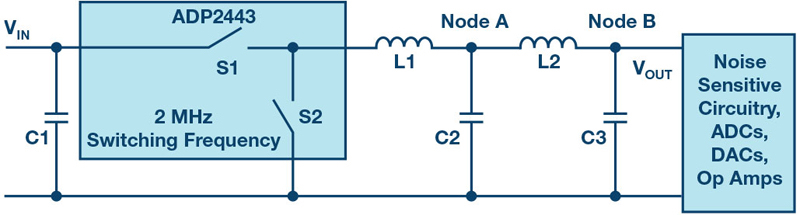
Figure 1. Buck regulator to power noise sensitive loads with an LC filter on the output
Different filtering techniques can be used to reduce the noise of a switching regulator. One that works especially well is an LC filter with an inductor in series with the power flow and a capacitor from the filtered voltage to ground. This type of LC filter creates a double pole in the frequency domain. Depending on the values for L and for C, the corner frequency — in this case, the double pole — can be set in a way to reduce the noise from the switching frequency and the switching transition frequency of a switch-mode power supply. The additional LC circuit functions as a low-pass filter.
When there is a noise issue in sensitive electronic equipment powered by a switch-mode power supply, a filter consisting of L2 and C3 can often be used (Figure 1). The output voltage of the power supply is being filtered by the LC filter. High frequency noise coming from the switching frequency, usually between 500 kHz and 3 MHz, and from the switching transition frequency, usually between 50 MHz and 200 MHz, is attenuated.
The location of the additional filter in the circuit is very important for successful filtering. Intuitively, one would put this filter between the output of the switch-mode power supply and the sensitive load. Such a sensitive load may be a high resolution ADC, DAC, a low signal op amp, or a sensitive VCO or PLL for RF circuitry. Any ripple voltage on the output of the buck regulator will be attenuated by the additional filter. While ripple voltage appears in node A (Figure 1), noise will be much lower in node B.
However, if the switch-mode power supply happens to be a buck regulator, and the additional LC filter is at the input of the switching regulator rather than the output, greater noise reduction is possible. This is shown in Figure 2. The reason for this is that a buck topology has relatively little noise on the output side. The inductor (L1 in Figure 2) is in series with the output path, (node A). This node will experience some ripple voltage, but the amplitude is usually only a few mV. The exact value depends on the switching frequency used, the input and output voltage values, and especially the selected component values of L1 and C2.
The input side of a buck topology, however, is very noisy. When switch S1 is off, no current flows into the buck regulator. When switch S1 is on, the full current flows into the circuit. The input capacitor C1 helps to reduce these intense current changes a bit. Still, the input side noise is much higher.
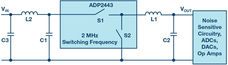
Click image to enlarge
Figure 2. Often an additional input filter reduces system noise much more than a filter on the output
Noise on the input of a buck regulator is not electrically connected to the sensitive load. However, in common circuits, there are many coupling mechanisms for such noise. The fast alternating currents on the input of the buck stage are often routed long distances on a circuit board. The changing currents can inductively couple onto other parts in the circuit and ultimately cause noise in the sensitive load circuitry.
The reason that an input side filter is more effective in reducing noise than an output side filter is specific to the buck topology. Other topologies, such as a boost or flyback, result in high noise on the output side. As a result, an additional LC filter on the output side is essential for lowering noise.
It is no secret that, when powering sensitive loads, additional filtering of a switch-mode power supply makes a lot of sense. Noise can be reduced effectively with such a filter. What many designers do not realize is thatin some situations, especially with buck regulators, it is critical to filter the input side for the best performance. Intuitively one would first look at the node between the buck regulator and the load that is being powered.
As explained in the article, this is a case where our intuition does not guide us to the best solution. Always look at the nodes where alternating currents, also called hot loops, occur and put additional filtering right there. Switching noise is then effectively reduced.
About the Author
Frederik Dostal studied microelectronics at the University of Erlangen-Nuremberg, Germany. Starting work in the power management business in 2001, he has been active in various applications positions including four years in Phoenix, Arizona, working on switch-mode power supplies. He joined Analog Devices in 2009 and works as a power management technical expert for Europe. He can be reached at frederik.dostal@analog.com.