System-Level Approach Enables the Design of Precision, High Density, Isolated Analog Output Module for Process Control
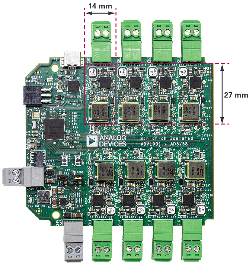
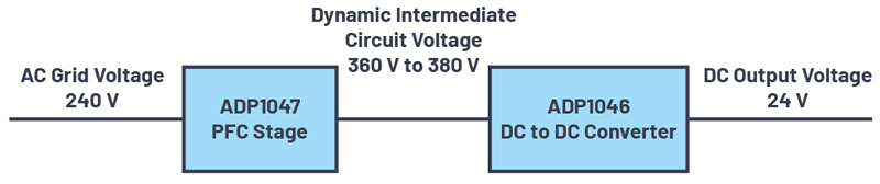
Figure 1. AD5758 and ADP1031 8-channel board
When designing channel-to-channel isolated analog output modules for process control applications, such as programmable logic controller (PLC) or distributed control system (DCS) modules, the main trade-off is usually between power dissipation and channel density. As module sizes shrink and channel densities increase, the power dissipation per channel must decrease to accommodate the max power dissipation budget for the module. Higher channel density also means that there is less PCB real estate available for each channel.
System-Level Solution
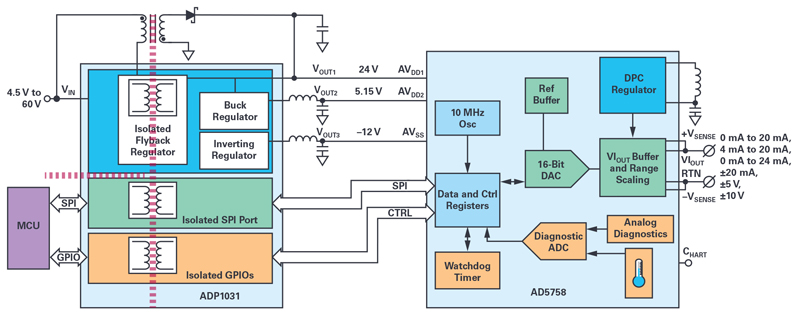
Figure 1 shows the AD5758 and ADP1031 system solution that solves both the power dissipation and space challenges, allowing a high level of integration. This design note shows how an 8-channel module with less than 2W of power dissipation for all channels can be produced in a compact form factor.
The ADP1031 solves the isolation and size challenges, providing 300 V basic isolation for power and data, while the AD5758 provides a low power dissipation, precision, configurable current or voltage output channel.
Integrated, Isolated Power and Data
Using ADI’s patented i Coupler® technology, the ADP1031 integrates three isolated power rails and SPI and GPIO data isolation in 7 mm × 9 mm. This high level of integration helps solve PCB real estate challenges as it consolidates all channel isolation requirements into a small area on the PCB.
Click image to enlarge
Figure 2. ADP1031 block diagram
Low Power Dissipation
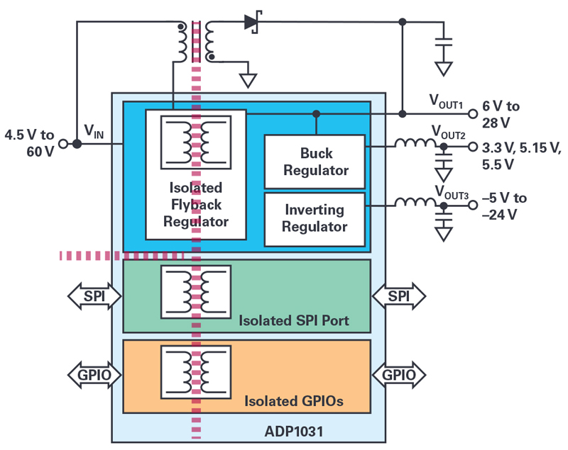
The AD5758 implements a technique called dynamic power control (DPC) to minimize power dissipation in the module under worst-case operating conditions when the part is configured for current output. It does this by continuously tracking the output voltage and reducing the power supply to the output driver to the minimum required to maintain the output load current — implemented via an integrated, programmable, high efficiency buck converter. When DPC is enabled for current output modes, the AD5758 automatically adjusts the DPC voltage to minimize power dissipation under all load conditions.
The ADP1031’s design is optimized to provide efficient isolated power for the AD5758 under worst-case load conditions so that the total channel power dissipation is minimized. The high speed SPI channel integrated into the ADP1031 is also designed to reduce power dissipation when active and enters a low power state when inactive.
Click image to enlarge
Figure 3. AD5758 block diagram
Isolation Flyback Transformer
Because the ADP1031 integrates the feedback channel, the design of the flyback transformer is simplified as a single primary and secondary winding is all that is required. This means the transformer form factor can be smaller while still meeting efficiency and isolation requirements. The recommended transformer for the ADP1031 has a footprint size of 8.6 mm × 8.26 mm and is less than 9.7 mm tall. A list of recommended transformers can be found in the ADP1031 data sheet.
Solution Size
The high level of integration allows each isolated channel to fit in an area of less than 400 mm2 on a two-sided PCB. This includes all associated passive components and isolation spacing.
Flexible Precision Channel with Diagnostics and HART Connectivity
The AD5758 includes advanced diagnostics to quickly detect incorrect behavior and faults.
Error flags are stored in two registers: a digital diagnostic results register and an analog diagnostic results register, for the on-chip digital and analog diagnostic features, respectively. Some of the key diagnostics are:
- Watchdog timer error
- SPI CRC error
- Invalid SPIaccess
- SCLK counterror
- Calibration memory CRC error
- Output overvoltage error
- Voltage output short-circuit error X Current output open-circuit error
- Overtemperature error
- Internal supply error
- DPC error
For a complete list of diagnostics, see the AD5758 data sheet.
The AD5758 also incorporates a 12-bit ADC to provide diagnostic measurements on user-selectable nodes, such as internal supplies and grounds, internal die temperature monitors, and internal references.
The AD5758 has a CHART pin, onto which a HART® signal can be capacitively coupled. Once HART connectivity is enabled, the HART signal appears on the VIOUT pin. This functionality is only available when VIOUT is configured to output current.
EMC Performance
The AD5758 incorporates line protectors on all pins that may potentially be connected to screw terminals (VIOUT, +VSENSE, and −VSENSE). The line protectors protect these pins from positive and negative voltages up to ±38 V by limiting the voltage internally to the VDPC+ and AVSS rails. If a voltage outside of these limits is detected on the VIOUT pin, an error flag is set, which can be read back over the SPI port.
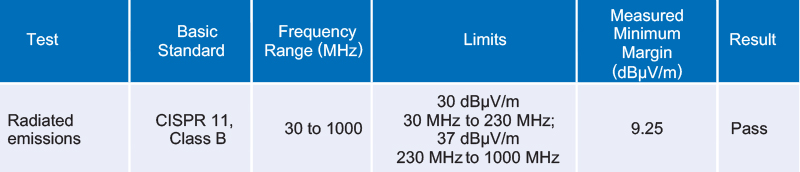
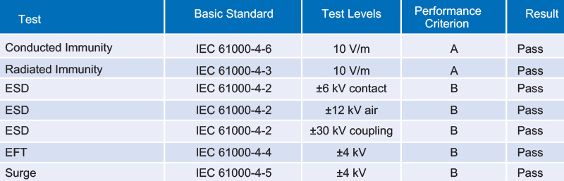
Extensive EMC testing has been completed on the AD5758 and ADP1031 system. See Table 1 and Table 2 for a summary of the test results.
Click image to enlarge
Table 1. Emissions Performance Summary
Click image to enlarge
Table 2. Immunity Performance Summary
System Applications Diagram
Click image to enlarge
Figure 4. System connection diagram.
Click image to enlarge
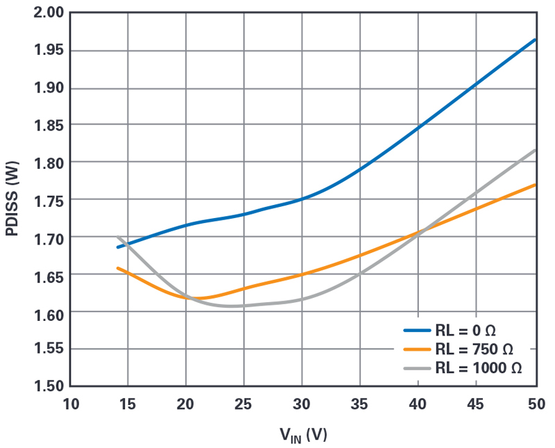
Figure 5. 8-channel module power dissipation vs. supply voltage and load.
Conclusion
The AD5758 and ADP1031 system-level solution enables a robust, compact, 8-channel, channel-to-channel isolated analog output module, which achieves best-in-industry power dissipation of less than 2 W for all eight channels operating under worst-case power dissipation conditions.