System-Level Approach to Software Configurable I/O Channels
A software configurable I/O device and its dedicated isolated power and data solution to solve design challenges in system-level industrial application designs.
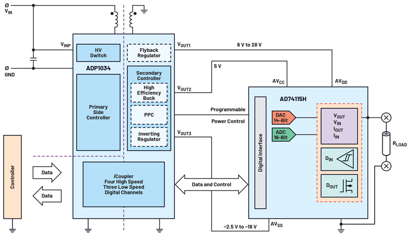
Figure 1: An ADP1034 and AD74115H circuit diagram
When designing system-level, isolated I/O solutions for industrial applications, such as process control, factory automation, or building control systems, there are many areas to consider. These include power dissipation, data isolation, and form factor. Figure 1 shows the system solution that solves power, isolation, and area challenges using the AD74115H and the ADP1034 in an isolated single-channel software configurable I/O solution.
System-Level Solution
The ADP1034 is a high-performance, isolated power management unit combining an isolated flyback regulator, an inverting buck boost regulator, and a buck regulator providing three isolated power rails and integrating seven low-power digital isolators. The ADP1034 also has programmable power control (PPC) functionality that is used for adjusting the voltage on VOUT1 on-demand through a single-wire interface. VOUT1 provides between 6V and 28V to the AD74115HAVDD powerrail. VOUT2 provides 5V to the AD74115H power rails AVCC and DVCC. It can also provide a supply voltage to an external reference if required. VOUT3 provides between –5V and –24V to the AD74115H AVSS power rail.
Power Dissipation and Optimization
When designing channel-to-channel isolated modules, the main trade-off is usually between power dissipation and channel density. As module sizes shrink and channel densities increase, the power dissipation per channel must decrease to accommodate the maximum power dissipation budget for the module. In this case, the module is defined as the ADP1034 and AD74115H, which when combined provide isolated power, data isolation, and software configurable I/O functions.
What makes the AD74115H and ADP1034 an optimum low power solution is the introduction of integrated PPC functionality. PPC gives the user the ability to adjust the VOUT1 voltage (AD74115H AVDD supply voltage) on-demand. This method minimizes power dissipation in the module under low load conditions, particularly in current output modes.
When using the PPC functionality, the host controller in the system sends the required voltage code via SPI to the AD74115H, which is then passed to the ADP1034 via a one-wire serial interface (OWSI). The OWSI has CRC implemented to provide robustness against EMC interference that may be present in harsh industrial environments.
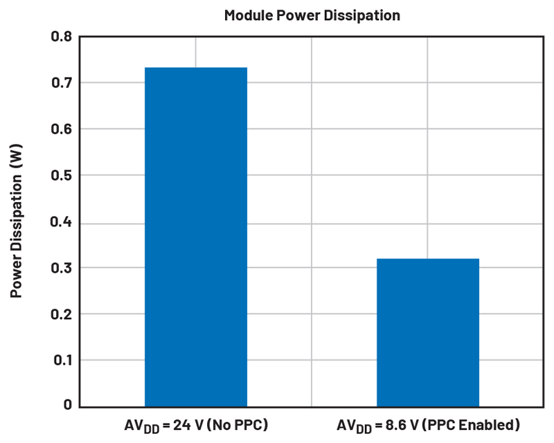
If we look at the example power dissipation calculation, we can see that if AVDD= 24 V and the load is 250 Ω, for a current output of 20 mA, there will be atotal of 748 mW dissipated in the module. When we use PPC to drop the AVDD voltage to 8.6 V (load voltage + headroom), there is ~348 mW dissipated in the module. This reveals a power saving of 400 mW within the module.
Example Power Dissipation Calculation
In Example 1 and Example 2, the current output use case is selected and is driving a 20 mA output. The load is 250 Ω and the ADC is enabled and converting the default measurement configuration at 20 samples per second.
Example 1 (NoPPC):
AD74115H Output Power = (AVDD = 24V) × 20mA = 480mW
AD74115H Input Power = AD74115HQUIESCENT (206 mW) + ADC Power (30mW) + 480 mW = 716 mW
Module Input Power = 716mW + ADP1034 Power (132 mW) = 848 mW
Load Power = 20 mA2 × 250 Ω = 100 mW
Total Module Power = (Module Input Power – Load Power) = 748mW
In Example 2, we can see that when the PPC functionality is enabled to reduce AVDD to the required voltage (20mA × 250Ω) + 3.6V headroom = 8.6V then the power dissipated in the module drops to 348 mW.
Example 2 (PPC Enabled):
AD74115H Output Power = (AVDD = 8.6V) × 20mA = 172mW
AD74115H Input Power = AD74115HQUIESCENT (136 mW) + ADC Power (30 mW) + 172 mW = 338 mW
Module Input Power = 338 mW + ADP1034 Power (100 mW) = 448 mW
Load Power = 20mA2 × 250Ω =100 mW
Total Module Power = (Module Input Power – Load Power) = 348 mW
Figure 2 shows the measured power dissipated on the AD74115H applications board at 25°C. The measurement shows the power dissipated is marginally lower than the calculated power dissipation. This will vary slightly from device to device.
Click image to enlarge
Figure 2: Measurement data 20 mA into 250 Ω load, AVDD = 24 V, AVDD = 8.6 V (PPC used)
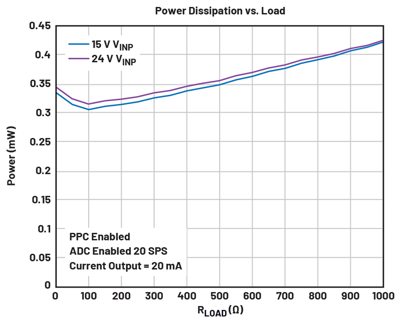
Figure 3 shows the module (ADP1034 and AD74115) power dissipation using PPC (optimized AVDD was programmed for each load resistor value) vs. different load resistor values. Two different voltages were applied to VINP of the ADP1034 (15 V and 24 V) to show the efficiency of the ADP1034. Measurements were taken at 25°C.
Click image to enlarge
Figure 3: Power dissipation vs. RLOAD at 20 mA output
Digital Output Use Case
In industrial applications, digital output is recognized as the most power-demanding use case. The AD74115H supports internal and external sourcing and sinking digital output. The ADP1034 can source enough power for the internal digital output function, capable of sourcing or sinking up to 100mA continuous current. In this case, the digital output circuitry supply DO_VDD is connected directly to AVDD. For currents higher than 100 mA, the external digital output function must be used, which requires an additional power supply connected to DO_VDD.
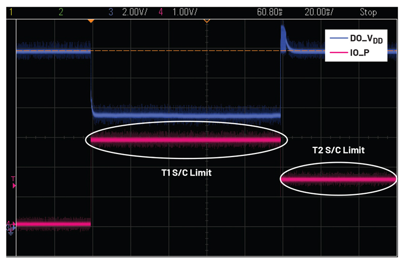
Internal Digital Output Use Case Timeouts
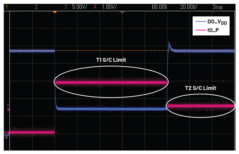
To support charging of capacitive loads on initial power-on, a higher short circuit current limit (~280 mA) can be enabled for a programmable amount of time, T1, while using the internal digital output use case. A second short-circuit limit (~140 mA) is deployed once the T1 time has elapsed. This is a lower current limit and is active for a programmable duration of time, T2. As more current is demanded from the system during these short circuit conditions, care must betaken to ensure the ADP1034 VOUT1 voltage doesn’t dip. To ensure there is no dip, a voltage of 24 V is recommended as the system supply voltage to ADP1034 for a required DO_VDD of 24 V. This is a typical required voltage for a 24 V relay. In the case of a 12 V relay, a minimum system supply voltage (ADP1034 VINP) of 18 V is recommended to ensure enough current can be sourced to the load.
Figure 4 and Figure 5 show the DO_VDD vs. T1 and T2 short circuit limits proving the stability of sourcing high current with the ADP1034.
Click image to enlarge
Figure 4: System supply = 24 V, DO_VDD voltage = 24 V
Click image to enlarge
Figure 5. System supply = 24 V, DO_VDD voltage = 12 V
Data Isolation and Solution Size
Using Analog Devices’ iCoupler technology, the ADP1034 integrates three isolated powerrails including SPI data and three GPIO isolation channels in a 7 mm × 9 mm package. This high level of integration helps solve PCB real estate challenges as it consolidates all channel isolation requirements into a small area on the PCB. Power savings are also realized. The controller side on the ADP1034 puts the other SPI isolator channels in a low power state when the channels are not in use. This means that the channels are only active when required. The three isolated GPIO channels are used to isolate the RESET, ALERT and ADC_RDY pins of the AD74115H, thus providing all the isolation requirements of the AD74115H without the added cost of an additional isolator IC.
Conclusion
Designing a low-power, small form factor channel-to-channel isolated I/O solution can be a challenge. The ADP1034 and AD74115H system-level solution simplifies the challenge with the high level of integration and system-level design approach. With a single IC providing three isolated power rails from a single system supply and integrated data isolation, the BOM cost reduces significantly. Coupled with the flexibility of the AD74115H, the system design will satisfy most I/O industrial applications.