Dealing with the challenges associated with DC and pulsed I V measurements
Characterizing the latest generation of wide-bandgap power semiconductor devices fully demands making the various measurements while the device is in its on-state, its off-state, and while it’s transitioning from one state to another. Although capacitance-voltage (C-V) measurements are increasingly important because of their usefulness in predicting certain dynamic characteristics of devices, such as switching time and gate charge, they are too complex a topic to address in an article of this length.
One of the most significant trends in power semiconductor characterization over the last decade is the growing use of source measure unit (SMU) instruments rather than separate power supplies and meters. Several factors contribute to this growing preference; for example, using an SMU instrument at each device terminal offers the flexibility needed to measure a variety of characteristics without the complication of reconfiguring cabling to instrumentation for every measurement. SMUs also offer tight timing integration. A growing number can be programmed to source high levels of current or voltage or measure both. Other designs can source and sink current and voltage, which offers speed and throughput advantages when it’s necessary to discharge system capacitances. Many SMU instruments also offer the advantage of a wide dynamic range.
On-state measurement challenges
Given that power devices often carry tens to hundreds of amps, they are typically characterized using pulsed DC stimulus to minimize power dissipation in the device itself. Obtaining reliable pulsed measurements demands careful attention to the test setup, making quality connections, and employing techniques that combat common instability issues when characterizing high gain power devices.
Optimizing pulsed DC measurements requires using low inductance; low resistance cabling that is sized to carry the circuit’s maximum test current. This not only helps minimize ringing and overshoot in the pulse shape but also helps ensure the correct signal is present at the device under test (DUT). Given that tens of amps may be involved, use 4-wire sense mode to ensure the voltage at the DUT is accurate.
The Force lines for the high current SMU should always carried separately to the DUT. It is best to connect the high current SMU LO and the lower power Gate SMU LO only at the FET’s source terminal or IGBT emitter terminal. To ensure the correct gate voltage, connect the SMU to the gate using 4-wire connections.
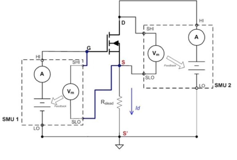
Figure 1 illustrates a lower power SMU instrument connected to the gate and a high current SMU instrument connected to the drain using 4W connections. Using 4-wire sensing at the gate terminal compensates for any voltage error due to the large current flowing through the lead resistance at circuit common.
Click image to enlarge
Figure 1. Using 4-wire sensing on the gate SMU allows it to measure and correct the output voltage based on the voltage at the actual device terminal
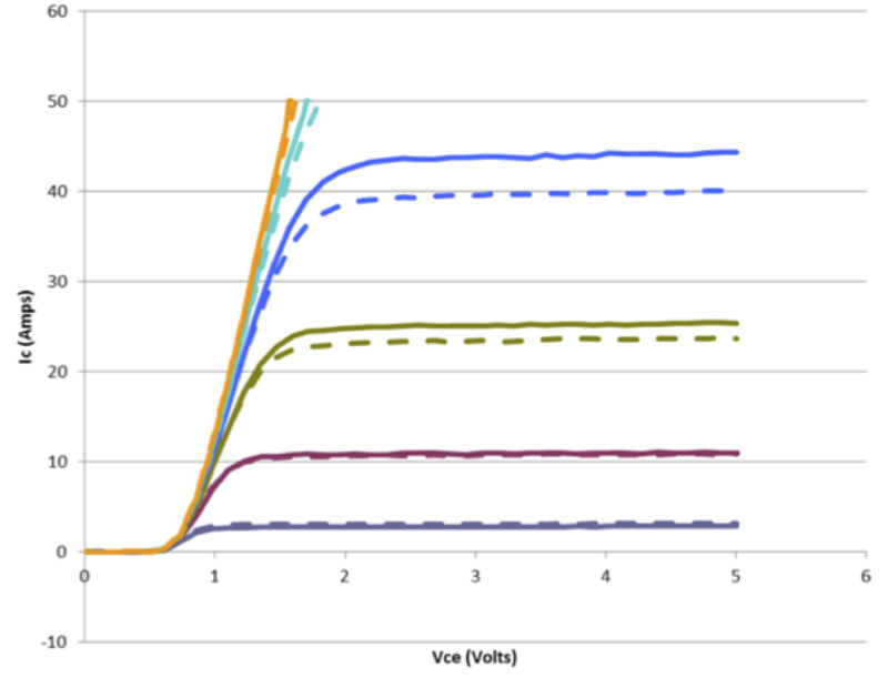
Power devices have high gain, so small changes in gate voltage can result in large changes in current at the MOSFET drain or IGBT collector terminal. This fact underscores importance of making correct connections. Note the significant differences in the IGBT collector current shown in Figure 2. When the gate SMU is connected correctly (solid lines) vs. incorrect connections (dashed lines) because the intended gate voltage was not the actual voltage in the incorrect connection scenario. Even when using 4-wire connections, it’s recommended that the Force LO from the drain/collect SMU be conducted through a signal line separate from gate SMU LO. Such a connection ensures that high current pulses will not affect gate SMU accuracy.
Click image to enlarge
Figure 2. In this family of curves, solid lines are the results when the gate SMU is properly connected, and dashed lines are the results with the gate SMU improperly connected. Note that collector current is higher with the gate SMU connected to the device properly
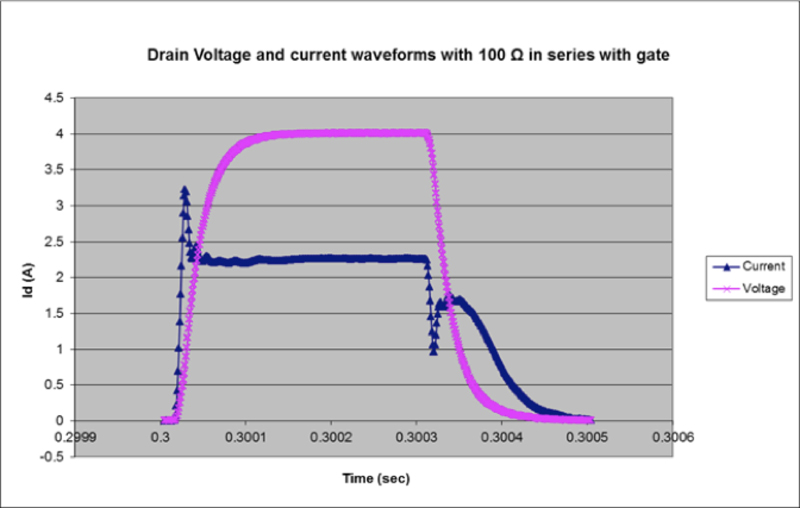
When making pulse measurements on power devices, keep in mind that the desired result is still a DC measurement; the objective is to find the DC value at the top of the pulse after settling (see Figure 3). The fidelity of the pulse, therefore, is critical to obtaining reliable, repeatable measurements.

Click image to enlarge
Figure 3: The objective is to find the DC value at the top of the pulse after settling
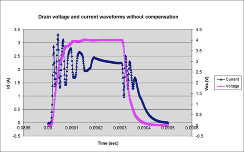
High gain and high speed transistors often self-oscillate during pulses. Any perturbations in drain voltage as the device turns on are injected into the gate and then fed back to the drain, resulting in oscillation (see Figure 4). Interactions between the test instrument and the DUT can also sometimes result in oscillation.
Click image to enlarge
Figure 4: The device turns on are injected into the gate and then fed back to the drain, resulting in oscillation
The first step in combating oscillation is to add a resistor in series with the gate SMU instrument. It’s important to choose a resistor value that’s large enough to dampen oscillation but not so large that it has a significant impact on the DUT’s switching time. An appropriate gate resistor value typically lies between a few ohms and 100 ohms and may vary from device to device. Pulse ringing may not disappear completely. The important point is to have a flat portion of the pulse from which to obtain a stable measurement (see Figure 5). An SMU instrument designed with voltage and current digitizers is essential for inspecting pulse fidelity.
Click image to enlarge
Figure 5: The important point is to have a flat portion of the pulse from which to obtain a stable measurement
Off-State Characterization Challenges
Off-state measurements are typically made at or near a DUT’s maximum voltage. For power semiconductor devices, this can mean sourcing a wide range of values, some up to thousands of volts. In a high voltage test environment like this, it’s essential to be vigilant about personal safety, overvoltage protection for instruments, and system capacitance issues.
Working safely in a high-voltage test environment
High voltage test environments can pose significant risks of electric shock for both system users and those working nearby. To minimize these risks, the use of high voltage cabling and probe tips rated for the system’s test voltage is essential. The chuck used must also be rated for high voltages. Modern test instrumentation and text fixtures typically include safety interlocks designed to protect users from coming in contact with dangerous voltages. Attempting to disable or go around these safety features creates an enormous risk of injury or death.
Any charged elements or capacitances in the system should be fully discharged before the user touches system components or connections. It is a good practice to use a discharge probe to discharge these capacitances manually before making setup changes or adjustments.
Protecting lower voltage instrumentation in the test systems
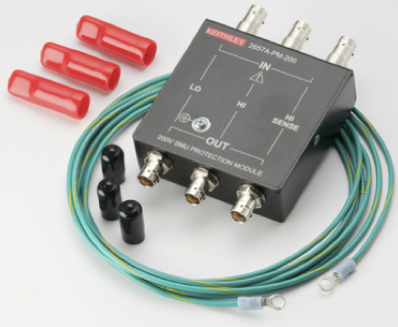
When being used in the same test system as high voltage instrumentation, lower voltage or lower power instrumentation is susceptible to damage, particularly in applications that involve testing at or near a device’s breakdown voltage. If breakdown occurs, high voltages can appear at the terminals of lower voltage instruments, which can damage or destroy them. When designing protection, carefully consider all potential modes of device failure and how other instruments in the system can be affected when a breakdown occurs. An overvoltage protection module (see Figure 6) can help prevent a low voltage SMU from being damaged by exposure to a higher voltage SMU.
Click image to enlarge
Figure 6. Overvoltage protection module
Cable capacitances, parasitic capacitances of the device, and other capacitances in the system can extend settling time significantly in high resistance circuits. Make sure that the current limit of the voltage source or current source value is high enough to charge system capacitance in the time expected for the measurement.
Accounting for system capacitance issues
The amount of capacitance in the system directly affects settling time because that capacitance must be charged or discharged at the start and conclusion of each test. When stepping the voltage source or SMU instrument, ensure it has sufficient current capability to charge the system capacitance.
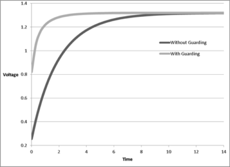
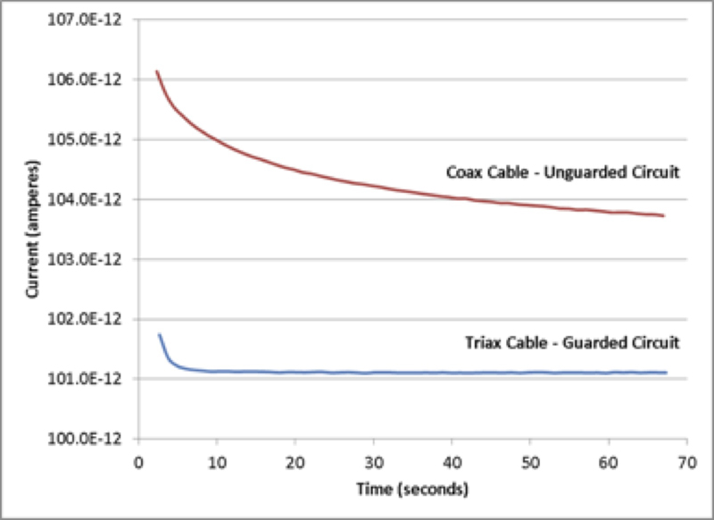
Cable capacitance is just one component of system capacitance, but it can quickly add up to hundreds of picofarads. Using triaxial cable allows the use of a guard. Guarding drives the inner shield of the triax cable at the same potential as the center conductor, which essentially eliminates the need to charge the cable capacitance and produces much faster settling times (see Figure 7a & b).
Clcik image to enlarge
Figure 7a illustrates the difference in speed at which the voltage rises to the SMU instrument’s programmed output voltage when triaxial cabling is used versus when coaxial cabling is used.
Click image to enlarge
Figure 7b shows how using guarded triax cabling supports faster settling and lower current measurements.
Be aware of the currents generated when system capacitances are discharged. This is of particular concern during unexpected and rapid discharge events, such as during device breakdown. Rapid changes in device impedance can produce very large capacitive discharge currents that can destroy devices or damage instrumentation or accessories. To limit capacitive discharge currents, insert resistance in series with the DUT. Be sure the resistor used is rated for maximum test voltage so it won’t be damaged when the high voltage is applied.