press x to close
Author:
Alex Lidow Ph.D., Robert Strittmatter Ph.D., Shengke Zhang Ph.D., and Alejandro Pozo Ph.D. Efficient Power Conversion
Date
03/02/2020
 PDF
PDF
Click image to enlarge
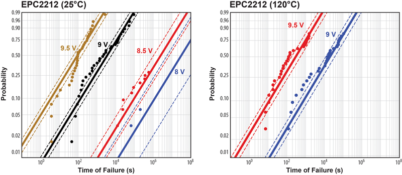
Figure 1: Weibull plots of gate-to-source failures of EPC2212. Note that very few failures occur even at 8 VGS , yet the device has a maximum VGS rating of 6 V. The data on the left is at 25oC and the data on the right is at 120oC
Standard qualification testing for semiconductors typically involves stressing devices at-or-near the limits specified in their data sheets for a prolonged period of time, or for a certain number of cycles. The goal of qualification testing is to have zero failures out of a relatively large group of parts tested.
This type of testing is inadequate since it only reports parts passed a very specific test condition. Perhaps parts would fail more frequently at a different operating point, one that isn’t at-or-near the data sheet limit. Perhaps the parts would fail at an alarming rate just past the data sheet limits.
By testing parts to the point of failure an understanding of the amount of margin between the data sheet limits can be developed, but more importantly, an understanding of the intrinsic failure mechanisms can be found. By knowing the intrinsic failure mechanisms, the root cause of failure, and the device’s behavior over time, temperature, electrical or mechanical stress, the safe operating life of a product can be determined over a more general set of operating conditions (For an excellent description of this methodology for testing semiconductor devices see reference).
What are the key stress conditions encountered by GaN power devices and what are the intrinsic failure mechanisms for each stress condition?
As with all power transistors, the key stress conditions involve voltage, current, temperature, and humidity. There are, however, many ways of applying these stress conditions. For example, voltage stress on a GaN FET can be applied from the gate terminal to the source terminal (VGS), as well as from the drain terminal to the source terminal (VDS). For example, these stresses can be applied continuously as a DC bias, they can be cycled on-and-of, or they can be applied as high-speed pulses. Current stress can be applied as a continuous DC current, or as a pulsed current. Thermal stresses can be applied continuously by operating devices at a predetermined temperature extreme for a period of time, or temperature can be cycled in a variety of ways.
By stressing devices with each one of these stress conditions to the point of generating a significant number of failures an understanding of the primary intrinsic failure mechanisms for the devices under test can be determined. To generate failures in a reasonable amount of time the stress conditions typically need to significantly exceed the data sheet limits of the product. Care needs to be taken to make certain the excess stress condition does not induce a failure mechanism that would never be encountered during normal operation. To make certain this is not the case, the failed parts need to be carefully analyzed to determine the root cause of their failure. Only by verifying the root cause can a true understanding of the behavior of a device under a wide range of stress conditions be developed.
Example number one: gate-source voltage stress
In figure 1 is an example of a Weibull plot of gate failures in an EPC2212 eGaN FET from Efficient Power Conversion (EPC). The vertical axis shows the cumulative failures for different stress conditions applied from gate-to-source. The horizontal axis shows the time to failure.
The plot on the left has different voltages at room temperature and the plot of the right shows two different voltages applied at 120 oC. Note that this device has a data sheet maximum gate voltage rating of 6 V, yet very few devices are failing even after many hours at 8 V.
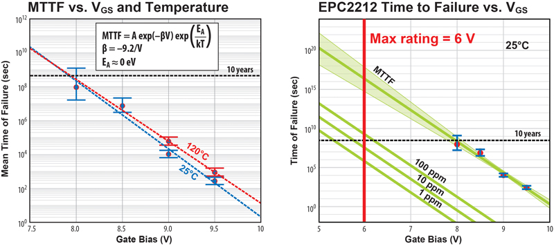
In figure 2, these data have been translated into failure rates. On the left is the mean time to failure (MTTF) for these same devices versus VGS at both 25 oC and 120 oC. On the right is a graph that shows the various probabilities of failure versus VGS at 25 oC. Note that the failure rate is not very sensitive to temperature, but is very sensitive to VGS.
Looking at the graph on the right, it can be seen that with a VGS of 6 V DC one could expect between 10 and 100 parts per million (ppm) failures in 10 years. The recommended gate drive voltage, however, is 5.25 V and the expected failure rate at that voltage is less than 1 ppm in 10 years.
Click image to enlarge
Figure 2: On the left is the mean time to failure (MTTF) for EPC2212 eGaN FETs versus VGS at both 25 oC and 120 oC. On the right is a graph that shows the various probabilities of failure versus VGS at 25 oC
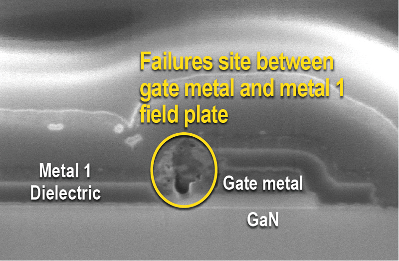
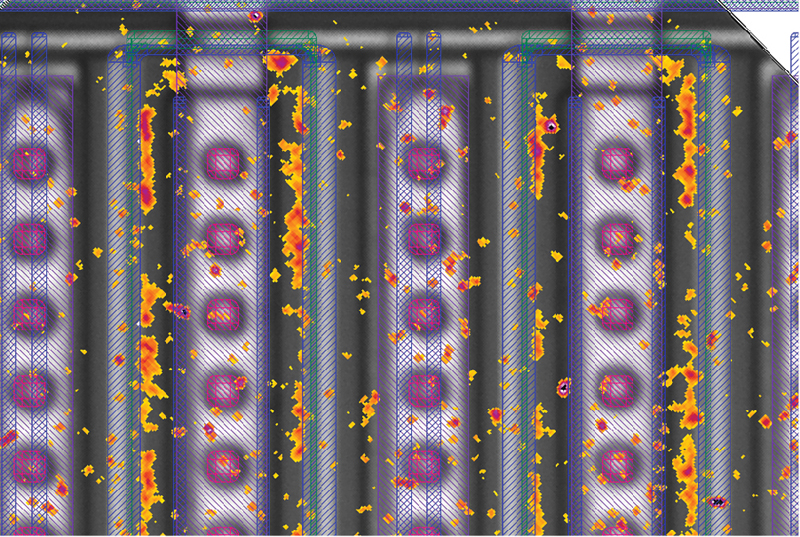
These conclusions are only valid if the primary failure mechanism is the same under all these conditions. In order to confirm this, failure analysis was performed on the failed parts and a uniform result was found, as shown in figure 3. Referring to the image in figure 3, the red circle shows that the failure site is between the gate metal and the metal 1 layer.
In the case of the EPC2212, these two layers are separated by a silicon nitride layer. It is this silicon nitride layer that failed, not any of the GaN layers beneath. Knowing this failure mechanism and understanding that it is consistent with time dependent dielectric failure mechanisms (TDDB) commonly found in dielectric layers in most semiconductors, the probability data in figure 2 to predict failure rates due to gate-source stress within data sheet limits can be used with confidence.
Click image to enlarge
Figure 3: Scanning electron micrograph (SEM) of the gate region of an EPC2212 eGaN FET. The red circle shows the failure site is between the gate metal and the metal 1 layer
Example number two: drain-source voltage stress
This same methodology can be applied to every other stress condition. For example, one common concern among GaN transistor users is dynamic on-resistance. This is a condition whereby the on-resistance of a transistor increases when the device is exposed to high drain-source voltage (VDS). The traditional way to test for this condition is to apply maximum-rated DC VDS at maximum rated temperature (typically 150 oC). If there are no failures after a certain amount of time – usually 1000 hours – the product is considered good.
The mechanism causing the on-resistance to increase is the trapping of electrons. Once an electron is trapped, it can no longer conduct and the resistance of the part in therefore increased. By applying DC VDS at maximum temperature, the electrons available to be trapped come from the drain-source leakage current, IDSS, which is typically in the micro-ampere range. In order to accelerate trapping, devices can be taken to voltages above their rated maximum, as shown in figure 4 for a fourth-generation, 100 V-rated EPC2212 eGaN FET.
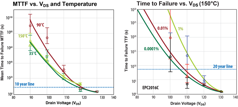
In figure 5 these data have been translated into time-to-fail graphs versus voltage and temperature. On the right side of the graph is shown the time for 1 ppm failures at the maximum rated VDS is over 10 years. What is unusual, however, is that the graph on the left shows that the failure rates are not very sensitive to temperature and that the failure rates, although extraordinarily low under all conditions, are higher at 90 oC than at either 35 oC or 150 oC. It will be shown later in this article that this can be explained by understanding that the primary failure mechanism is hot electron trapping.
Click image to enlarge
Figure 4: Weibull plot of EPC2212 eGaN FETs stressed under DC bias at various voltages. A failure is defined as exceeding data sheet limits
Click image to enlarge
Figure 5: The data in figure 4, as well as similar data taken at different temperatures, is translated into predictions of failure rates over time, temperature, and voltage
Figure 6 is a magnified image of an EPC2212 eGaN FET showing thermal emissions in the 1 – 2 µm optical range. Emissions in this part of the spectrum are consistent with hot electrons and their location in the device is consistent with the location of the highest electric fields when the device is under drain-source bias.
Click image to enlarge
Figure 6: A magnified image of an EPC2212 eGaN FET showing thermal emissions in the 1 – 2 µm optical range that is consistent with hot electron emissions
Knowing that hot electrons in this region of the device are the source of trapped electrons. A better understanding of how to minimize the dynamic on-resistance can be achieved with improved designs and processes. By understanding the general behavior of hot electrons, their behavior over a wider range of stress conditions can be generalized.
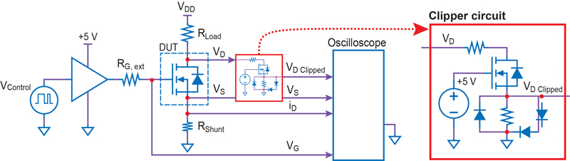
In addition, the trapping mechanism by providing more hot electrons can be accelerated. To do this, the circuit shown in figure 7 that pushes high IDSS through the device at maximum rated VDS was created. In other words, instead of just using the leakage current generated by DC bias at high temperatures as the source of electrons that can get trapped, orders of magnitude more trapping candidates by making a switching circuit such as shown in figure 7 can be generated. This circuit is like the inductive double-pulse testing specified by JEDEC JEP173.
Click image to enlarge
Figure 7: Inductive double pulse testing circuit consistent with JEDEC JEP173
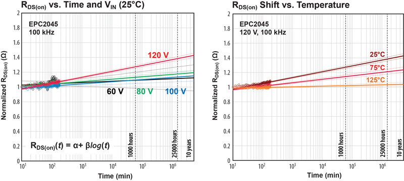
Figure 8 shows how the RDS(on) of a fifth-generation EPC2045 eGaN FET increases over time at various voltage stress levels and temperatures. On the left, the devices were tested at 25 oC at voltages from 60 V to 120 V (The device has a VDS(max) of 100 V). The horizontal axis is time measured in seconds, with the right side ending at 10 years.
The graph on the right shows the evolution of RDS(on) when biased at 120 V at different temperatures. The counter-intuitive result shows that the on-resistance increases faster at lower temperatures. This is consistent with hot carrier injection because hot electrons travel further at lower temperatures and therefore can get to different layers where they are more prone to become trapped. This suggests that traditional testing methods, whereby a device is tested at maximum voltage and temperature, may not be the best way to determine the reliability of a device.
Click image to enlarge
Figure 8: The RDS(on) of a fifth-generation EPC2045 eGaN FET over time at various voltage stress levels and temperatures. On the left the devices were tested at 25oC at voltages from 60 V to 120 V. The graph on the right shows the evolution of RDS(on) at 120 V at various temperatures
The results in figure 5 as well can now be better understood. As the device is heated under DC bias, the leakage current increases. The shorter travel distance of the hot carriers, however, counters this increase in available electrons such that the RDS(on) increase over time climbs from room temperature to 90 oC, but then starts declining at higher temperatures – another counter-intuitive result.
Summary
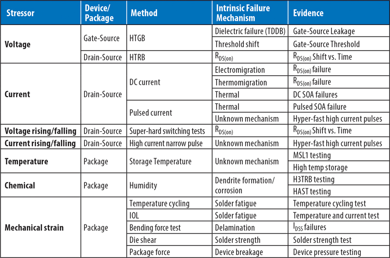
Table 1 shows the various stress conditions applied to eGaN FETs, the methods used to apply the stress, and the intrinsic failure mechanisms found. Tens of thousands of devices over a ten-year period, and five generations of technology, have been tested to develop this generalized understanding of the behavior of these devices over all these stress conditions. The result is that GaN is an extremely robust technology that continues to improve at a rapid pace. The question remaining is whether silicon MOSFETs can come close to matching the robustness of GaN?
Click image to enlarge
Table 1: Stress Conditions and Intrinsic Failure Mechanisms for eGaN FETs