Negative voltages are needed in many different applications, and the specifications for these voltages vary quite significantly
Most systems require multiple different voltage rails. Voltages below the system ground voltage, or zero voltage, are considered to be negative voltages. Such voltages are needed in many different applications. In power electronics, some switch types may not reliably be turned off if ground voltage is applied to the gate. A negative voltage, a few volts below ground, can solve this issue.
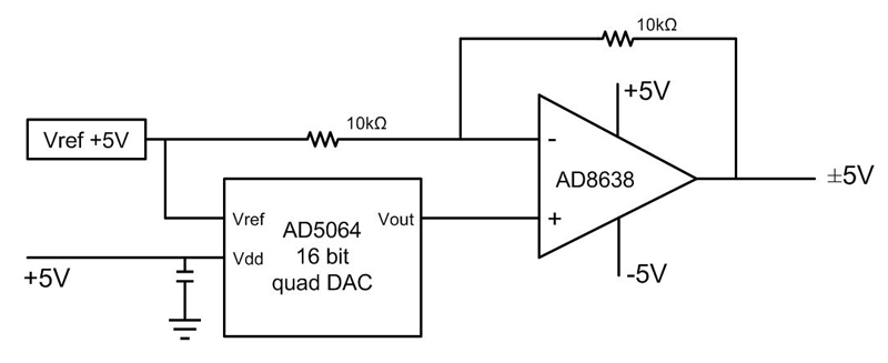
In the signal path of an instrumentation application, real world signals cannot easily be measured all the way to zero volts, if operational amplifiers measuring this real world signal are supplied by a positive voltage and zero volts only. Putting this operational amplifier between a positive voltage rail and a negative voltage rail allows for signals to be measured all the way down to zero volts. Figure 1 shows a 16 bit digital-to-analog converter (DAC) generating a bipolar output signal using an AD8638 operational amplifier. To power such a system, a low noise negative power supply is required.
Click image to enlarge
Figure 1. Negative supply voltage requirement in a DAC application generating bipolar signals
Generating a negative voltage using a transformer
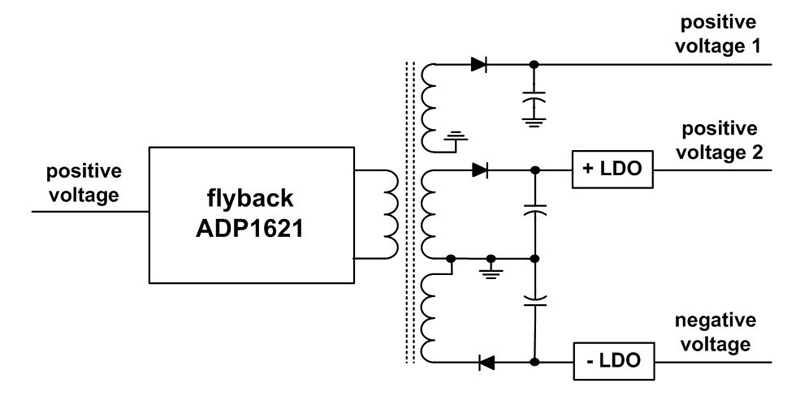
One of the easiest ways of generating a negative voltage is to add an additional winding to an existing transformer based power supply. By the transformer coupling, energy stored in a transformer core (flyback topology) or current flowing through the primary winding (forward topology) is injected into a secondary winding. This current flow can be biased to different reference voltages. By setting the directions of the secondary side winding turns, the direction of the diode and attachment of secondary side system ground, a negative voltage can be generated. Figure 2 shows a flyback topology with three secondary windings. One of them is generating a negative supply voltage.
Click image to enlarge
Figure 2. Generating a negative voltage using an additional winding on an existing flyback design
Such a concept makes a lot of sense if a transformer based topology is already used in a given system. Pulling in a transformer for the sole purpose of generating a negative voltage usually does not make economic sense. If however an additional secondary winding is added to an existing transformer based design, the generated negative voltage is not regulated by the converters feedback loop and this rail just sort of tags along. It is then not very tightly regulated and follows the load behavior on the main secondary side rail which is usually the one used to close the regulation loop of the flyback. This is why post regulation of the negative voltage rail with a negative linear regulator is usually necessary.
Generating a negative voltage using a charge pump
Charge pumps consist of capacitors and switches. Charge is stored on a capacitor and then by clever switching this charge can be added to different voltage rails, doubling voltages. This technique can also be used to invert positive voltages into negative voltages. Such converter designs are low cost and require little board space since no inductors are needed. The limitations are, that the maximum output current is typically limited to 100mA and also existing charge pump designs tend to be quite noisy. Especially as the load current is higher than a few 10s of mA (see Figure 3).

Click image to enlarge
Figure 3. Charge pump concept for inverting a positive voltage into a negative voltage
Generating a negative voltage using a Ćuk topology
A quite unique topology was named after Mr. Slobodan Ćuk who first presented the design. It is a topology which generates a negative output voltage from a positive input voltage. This topology does not require a transformer. While two inductors are necessary, they can be dual windings on a single core. Also a coupling capacitor in the power path is needed.
Figure 4 shows a Ćuk topology. For implementation of this circuit, a switching regulator or controller with a negative feedback voltage path is needed. Very few modern integrated DC to DC converter devices offer such a negative feedback pin. Certainly devices with a positive feedback pin may also be used as long as a discrete voltage inverter is added to the feedback path. This additional operational amplifier increases system cost but it also adds multiple components in the sensitive feedback path which often yield output voltage accuracy problems and may easily couple system noise into the feedback loop yielding noise on the output voltage.

Click image to enlarge
Figure 4. Ćuk topology generating a negative voltage from a positive supply
Generally, the Ćuk topology is very low noise. This comes from the fact that there is an inductor on the input side as well as on the output side. Current flow through an inductor cannot change instantaneously, thus input currents and output currents are very stable currents opposed to other switching regulator topologies.
Generating a negative voltage using an inverting buck-boost topology
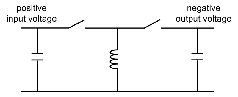
The inverting buck-boost topology is one of the basic three inductive switch mode power supply topologies. It requires only one inductor, two switches and an input and output capacitor. The other two topologies that also work with these basic components are the buck topology and the boost topology. The buck topology has the inductor on the output side, the boost topology has the inductor on the input side and the inverting topology has the inductor on neither the input nor the output side. The inductor is attached between the switch node and ground as can be seen in Figure 5.
Click image to enlarge
Figure 5. Inverting buck-boost topology generating a negative voltage from a positive supply voltage
The switch mode power supply IC that can be used for the inverting topology is any type of device intended for the buck topology. There are many such products available on the market. Using a buck regulator in an inverting buck-boost topology comes with one important challenge. The buck regulator used in an inverting buck-boost topology will generate a negative output voltage, which equals the buck regulators ground connection voltage. The output voltage of the buck regulator will then equal the system ground voltage.
This behavior is generally not an issue, however, the result is, that all support pins of the buck regulator are referenced to the buck regulator ground and not system ground. Since the buck regulator ground becomes the negative voltage, once the circuit is operating in steady state, some level shifting on pins such as a synchronization input, enable, tracking feature and many others need to be level shifted, so that the system signal for these pins are in reference to the buck regulator ground (the generated negative voltage) and not system ground.
The advantage of the inverting buck-boost regulator is that only very few power stage components are needed, the power conversion efficiency tends to be quite high and there are many controller ICs to choose from. As a disadvantage we can note the fact that the inverting buck-boost topology has no inductor on the input side and no inductor on the output side. Thus there are discontinuous currents on the input side and the output side. In noise sensitive applications, some additional filtering may be needed.
The reason for the name inverting ‘buck-boost’ topology is that the value of the input voltage may be higher or lower than the adjusted absolute of the negative output voltage. For example, a negative 12V can be generated from a positive 5V or 24V rail. This feature is used in some applications, which do not even require a negative voltage. For example, a string of LEDs can be driven with an inverting buck-boost topology with an input voltage higher or lower than the combined forward voltage drop of the LED string. The negative polarity of the generated output voltage can be addressed by flipping the LED string over.
Post-filtering negative voltages using a linear regulator
While linear regulators such as LDOs (low dropout linear regulators) cannot generate negative voltages from a positive voltage, they can drop a negative voltage to a lower negative voltage. They can either be used for regulating non-regulated voltages, often generated with an additional negative winding on a flyback transformer, or they can be used to filter existing negative voltage rails to generate ultra low noise negative supplies for noise sensitive applications.
For just a rough voltage stabilization a discrete negative linear regulator can be built with a transistor, a zener diode and a few resistors, when low drop-out, low noise, high power supply rejection ratio (PSRR) or a fast regulation loop for high DC accuracy of the output voltage is required, an integrated negative LDO s needed. Unfortunately, linear regulators intended for positive voltages will not work with negative supply voltages.
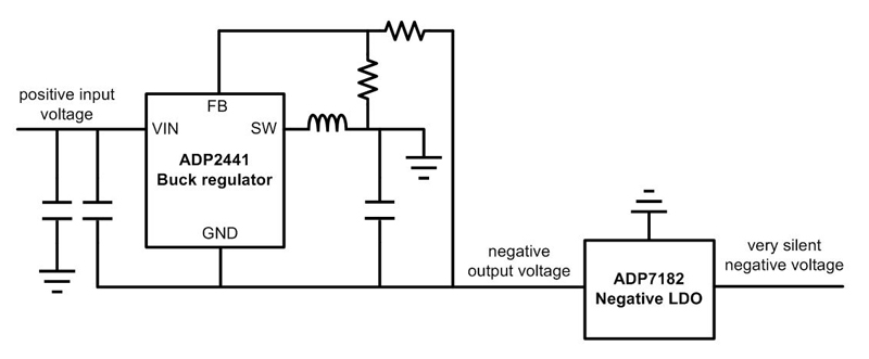
Negative linear regulators exist on the market, but there are not many. From the ones that are available, many were released to the market a long time ago, use old semiconductor processes and thus do not have state of the art electrical characteristics. Figure 6 shows the ADP2441 in the inverting buck-boost topology. The output is post filtered by a modern negative LDO from Analog Devices, the ADP7182 with an input voltage range all the way down to -28V and a maximum of 200mA output current. The power supply rejection ratio is -66dB at 10kHz, allowing for good ripple attenuation in low noise applications.
Click image to enlarge
Figure 6. Negative linear regulator used on the output of an inverting buck-boost topology
Circuit example using a dedicated inverting buck-boost converter
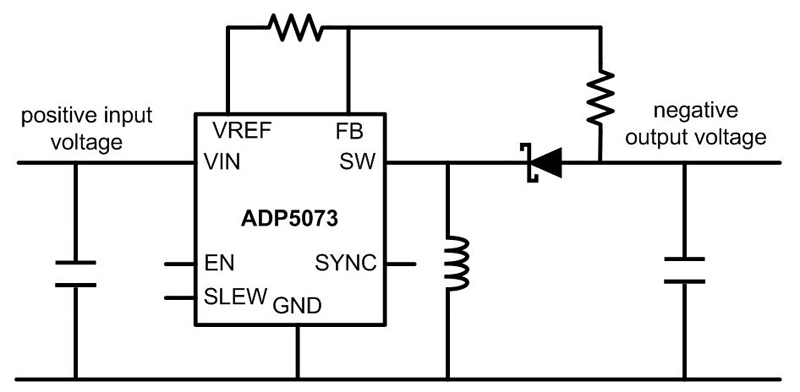
The concepts introduced above have been used for many years. However, recent developments yielded a few switch mode regulator ICs which are optimized to generate negative voltages. The ADP5073 is a specialized switching regulator IC intended for the inverting buck-boost topology. It has level shifting included, so that the enable pin is referenced to IC ground and system ground. This significantly simplifies sequencing requirements in a given system. Also it has a special SLEW rate feature implemented which helps significantly to reduce switching noise coming from an inverting buck-boost topology.
This slew rate pin can adjust the switching transition speed of the switching power supply. Fast switching transitions offer lowest switching losses, slowest speed offers lowest noise generation. There are three settings which can be chosen, allowing for an optimization of lowest noise and highest power conversion efficiency at a late point in the design process.
The ADP5073 can drive a maximum switch current of 1.2A. The maximum possible output voltage depends on the input to output voltage ratio. Figure 7 shows an example design of an inverting buck-boost power supply using the ADP5073 for low noise applications due to the SLEW pin function.