An update on the rate of adoption and the future of GaN power devices
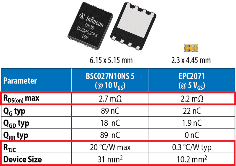
Table 1: GaN (EPC2071) vs. Silicon Comparison
The adoption of gallium nitride (GaN) in power devices has seen significant growth in recent years. In this article the various factors impacting the adoption of GaN are examined as well as how these challenges are being addressed and overcome. With over 14 years of volume production experience, EPC has identified key concerns voiced by customers which fall into the following categories:
1. Small size and thermal management: GaN devices can be 10 – 15 times smaller than the power MOSFETs they are replacing. This leads to challenges in manufacturing, as well as design, and with small size also comes the issue of thermal management.
2. Reliability concerns: Customers express concerns about the reliability of GaN power devices due to several factors, including the relative newness of the technology and its implications for long-term performance over the lifetime of their applications.
3. Ease of use: The higher speed of GaN devices, ranging from 10 to 100 times faster than traditional MOSFETs, has raised concerns about ease of use. Also, traditionally there has been less infrastructure in place to support gallium nitride devices though that is rapidly changing.
4. Cost: If the cost of new technology remains high, only niche applications will adopt it. As the cost of GaN crosses over the cost of silicon the ramp to mass adoption accelerates.
What about the small size? Table 1 shows a fifth generation GaN device, the EPC2071, that is about 10 mm2 against a benchmark silicon device that is about 31 mm2. The on-resistance of the MOSFET is about 20% higher than the GaN device. However, the die size of the GaN device is 3x smaller than the MOSFET. Despite that, the thermal resistance to the case is 70 times lower for the GaN device where you can dissipate heat in all directions. The ability to dissipate heat in all directions allows users to maximize the heat dissipation capabilities which is especially critical in high-power density designs. Additionally, simple and cost-effective thermal management strategies can further improve heat conductance to optimize thermal performance.
What about reliability? GaN devices have been in volume production for more than 14 years and have demonstrated very high reliability in both laboratory testing and in high-volume customer applications. Gallium nitride is a wide bandgap semiconductor, which means that there is a tighter chemical bond between the gallium and the nitrogen atoms than there is between silicon atoms in a silicon device. And that has been demonstrated to make the devices more rugged and reliable and less sensitive to thermal and radiation effects. Extremely conservative and rugged applications have adopted gallium nitride, including satellites, automotive, and solar. Solar is an extraordinarily demanding application because the equipment is sitting in a variety of very difficult harsh environments and must last 35 years in some cases. In our phase 15 reliability report we not only characterize the failure mechanisms of GaN but show how these mechanisms can be used to demonstrate reliability under application-specific mission profiles. EPC has undertaken extensive reliability testing to continue to understand the behavior of gallium nitride devices over a wide range of stress conditions. The results of these studies show that GaN is an extremely robust technology. The extraordinary lifetime capability of gallium nitride devices has shown to be much greater than power MOSFETs.
Are these devices easy to use? Admittedly, wafer level chip scale devices are smaller and require more precision handling tools. Also, the devices are 10x faster, which means that circuits designed with GaN are more sensitive to parasitics, particularly parasitic inductance. Therefore, a careful layout is very important.
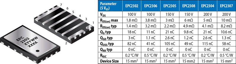
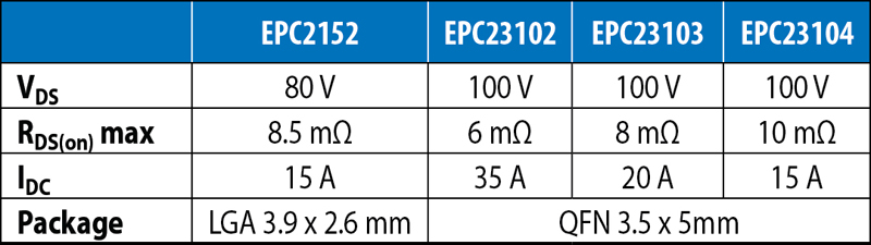
To further mitigate some of these handling concerns, EPC has introduced a family of power devices in packages that are familiar to designers used to packaged MOSFETs. Table 2 shows the spread of products available in Power Quad Flat No-Lead (PQFN) packages. This package adds no inductance, no electrical resistance, and is extraordinarily thermally efficient. It combines the tremendous advantage of low thermal resistance with the ease of PQFN assembly.
Click image to enlarge
Table 2: GaN FETs in 3 x 5 mm PQFN Package
To make GaN even easier to design and use, EPC has developed a family of integrated circuits. The monolithic power stages, shown in Table 3 include the high side and low side power devices integrated with their drivers, with a level shift, and with a sink boot to generate the high side gate signal. These solutions save design time but are also easier to use; all the designer needs is a logic-level input from the controller to get power output. Integration eliminates all the parasitic inductances that add to EMI and slow down the device. The resulting system is much smaller, and the efficiency is better.
Click image to enlarge
Table 3: GaN Integrated Power Stages
What about the cost? The misconception that GaN is more expensive than silicon persists. This is an outdated belief, which is simply not true. In 2023 at APEC and PCIM, EPC set up a booth and challenged people to bring their MOSFET part number and compare the pricing of the equivalent GaN FET. 60% of the people who took the challenge found that the price of the GaN FET was lower than the silicon MOSFET. Of the 24% that had higher prices they were very old, very cheap MOSFETs. When comparing GaN against state-of-the-art MOSFETs, the GaN FETs were always priced lower. To try this for yourself, go to the EPC cross reference search and enter a competitor’s part number to find a suggested replacement. Easily compare parametric differences without opening a single datasheet to identify the appropriate GaN FET to increase design efficiency.
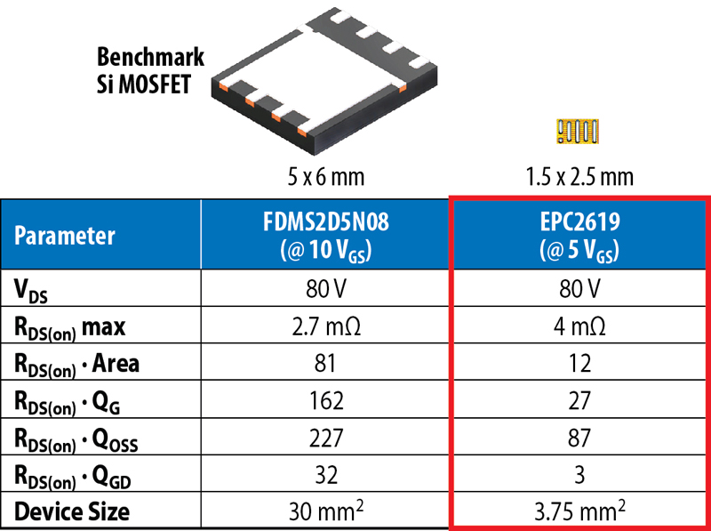
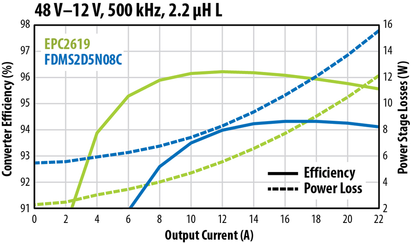
State of GaN today: Adoption is paced by customers perceptions and myths, most of which are based on older and earlier generations of GaN technology. EPC has released its first generation-six device with double the power density of prior generations. In applications this translates to higher efficiency and higher power output in a smaller footprint. Figure 1a shows a comparison of the Gen 6 device against the benchmark silicon MOSFET that is eight times larger in size. Figure 1b shows that despite the GaN device being 30% higher in on-resistance and significantly smaller, the efficiency of the device in a 48 V – 12 V buck converter at 500 kHZ is two percentage points higher and the losses are almost 40% lower.
Click image to enlarge
Click image to enlarge
Figures 4a & 4b: GaN vs MOSFET Comparison
In summary, the barriers to mass adoption of GaN power devices are rapidly falling, with advancements in size, thermal management, reliability, ease of use, and cost. Early adopters stand to gain a distinct advantage over competitors as GaN continues to redefine the landscape of power electronics.