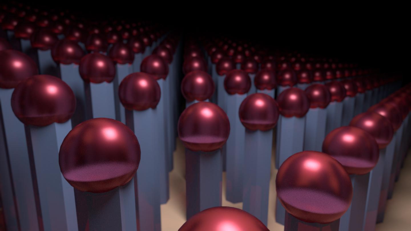
Nanowires have the potential to revolutionize the technology around us. Measuring just 5-100 nanometers in diameter (a nanometer is a millionth of a millimeter), these tiny, needle-shaped crystalline structures can alter how electricity or light passes through them.
They can emit, concentrate and absorb light and could therefore be used to add optical functionalities to electronic chips. They could, for example, make it possible to generate lasers directly on silicon chips and to integrate single-photon emitters for coding purposes. They could even be applied in solar panels to improve how sunlight is converted into electrical energy.
Up until now, it was impossible to reproduce the process of growing nanowires on silicon semiconductors - there was no way to repeatedly produce homogeneous nanowires in specific positions. But researchers from EPFL's Laboratory of Semiconductor Materials, run by Anna Fontcuberta i Morral, together with colleagues from MIT and the IOFFE Institute, have come up with a way of growing nanowire networks in a highly controlled and fully reproducible manner. The key was to understand what happens at the onset of nanowire growth, which goes against currently accepted theories. Their work has been published in Nature Communications.
"We think that this discovery will make it possible to realistically integrate a series of nanowires on silicon substrates," says Fontcuberta i Morral. "Up to now, these nanowires had to be grown individually, and the process couldn't be reproduced."
Getting the right ratio
The standard process for producing nanowires is to make tiny holes in silicon monoxide and fill them with a nanodrop of liquid gallium. This substance then solidifies when it comes into contact with arsenic. But with this process, the substance tends to harden at the corners of the nanoholes, which means that the angle at which the nanowires will grow can't be predicted. The search was on for a way to produce homogeneous nanowires and control their position.
Research aimed at controlling the production process has tended to focus on the diameter of the hole, but this approach has not paid off. Now EPFL researchers have shown that by altering the diameter-to-height ratio of the hole, they can perfectly control how the nanowires grow. At the right ratio, the substance will solidify in a ring around the edge of the hole, which prevents the nanowires from growing at a non-perpendicular angle. And the researchers' process should work for all types of nanowires.
"It's kind of like growing a plant. They need water and sunlight, but you have to get the quantities right," says Fontcuberta i Morral.
This new production technique will be a boon for nanowire research, and further samples should soon be developed.
EurekAlert!, the online, global news service operated by AAAS, the science society: https://www.eurekalert.org/pub_releases/2019-02/epfd-thg022019.php