The Ideal Package Design for Silicon Carbide and Wide-Bandgap Devices
An examination of the packaging trends and opportunities for power discrete and modules for the most demanding power switching applications
The introduction of improved semiconductor devices, namely wide bandgap types such as Silicon Carbide(SiC) and Gallium Nitride (GaN) will enable significantly higher performance power switching applications, especially in applications such as automotive traction inverters.
SiC power semiconductor technology offers significant advantages over traditional silicon-based devices in power applications requiring low losses, high frequency switching and/or high temperature environments. For example, the dielectric strength voltage of SiC is about 10 times greater than that of Silicon. Low losses are critical to the performance ratio and SiC technology can reduce the power loss by up to a factor of five.
Some of the advantages of these technologies have been demonstrated and deployed, especially with Silicon Carbide in standalone charging station applications (high voltage) and more recently in traction inverter assemblies (high temperature, high switching frequency), emerging as a true “killer application” in the realm of automotive electrification.
With the potential for drastically improved performance, a challenge for the industry remains. What new package innovations can be deployed to realize the full performance advantages of these promising semiconductor devices?
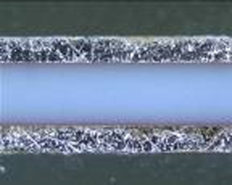
The first step in the evolution of improved power module package designs, even before the advent of SiC, involved the use of direct bonded copper on ceramic substrates, such as alumina and aluminum nitride to replace those made with pure copper. These ceramic substrates exhibit significantly lower coefficient of thermal expansion (CTE) characteristics, while still providing reasonable thermal conductivity.
As shown in Figure 1a & 1b, the CTE can be modified by adjusting the thickness of the copper relative to the thickness of the inner core alumina, for example, resulting in 7-9ppm/degree C, which provides a much better match for mounting low CTE semiconductor dies. By so doing, the total CTE mismatch - die to substrate – is now 3-7ppm, rather than 13-15ppm, which is the case for a semiconductor die mounted to a copper lead-frame. The use of direct bond copper (DBC) substrates is very common in multi-die power module systems today, but copper lead-frames are also selectively used ,especially with single die devices.
Click image to enlarge
Click to enlarge image
Figure 1a & Figure 1b. Variations in ceramic and copper thickness in DBC substrates
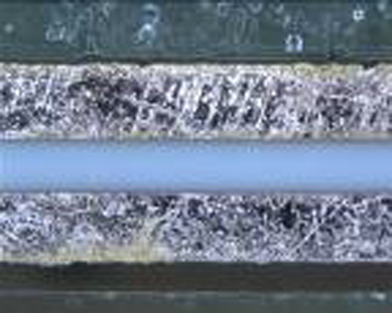
Another recent development is the use of aluminum as a metallization on ceramic – referred to as DBA. Vendors offering these materials claim improved thermal cycling performance compared to copper metallization.
As shown in Figure 2, the ceramic substrate topside metallization is etched to form a physical circuit, which can accept die attachment, followed by topside wire-bonds.
Click image to enlarge
Figure 2. Etched topside direct bond copper on ceramic substrate
ENIG substrate finishes are also common, which provides robust surface protection prior to the die attach process, which often consists of solder reflow. Typical solders include the use of high lead for the die attach, and lower melting temperature solders deployed for the substrate bottom attach to the module heat spreader.
In the lead free arena, SnSbX alloys have found application due to their superior creep resistance and acceptable melt temperatures. Both step soldering and one step soldering processes are common, usually in a reduction environment, and sometimes with the aid of vacuum, to remove voids. Fixtures are deployed to control bondline thickness and to minimize die tilt. The use of solder preforms with built in bondline control features, such as Alpha’s TrueHeight product are also used as an alternative to extensive fixturing.
These types of power modules, constructed as described here, are common for all types of high power AC motor control applications, with a good example being electric train propulsion.
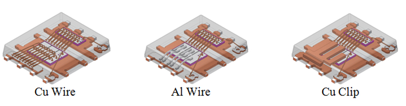
In a similar manner, single die or double die packages such IGBT Diode pairs, have historically used a heavy copper leadframe, and topside wirebonds for power connections as well as control.
As shown in Figure 3, the aluminum bondwires can be replaced with a copper clip for improved die cooling. This configuration also provides improved thermal cycling performance.
Click image to enlarge
Figure 3. Aluminum wirebond topside power connections (left) and improved cooling with a copper topside clip (right)
As with single die packages, modules that replace the aluminum wirebonds with a more robust topside connection realize additional die cooling, greater current density, and improved power cycling. Double sided cooling of IGBT Diode modules was proposed more than 15 years ago (#1), and has found deployment in a number of automotive traction inverter assemblies used with hybrid electric vehicles. In modules that are based on DBC alumina or aluminum nitride, the topside connections are also achieved with the same materials, creating a sandwich architecture. Typical implementations, depending on topside die contact area, can result in a 30% decrease in the thermal resistance of the module.
Double sided cooling modules may need functions that can provide clearance for non- power oriented wirebonds, such as the small gate and current sense pads. In these cases, or when it is necessary to ensure a minimal air gap between substrates in higher voltage applications, spacers are used. The spacers can be constructed from thermally and electrically conductive materials, such as copper, but since the die sizes of conventional silicon can be quite large – 12mm x 12mm – there is concern about CTE mismatch when using large copper pieces connected with only a relatively thin solder bondline between the copper and the die surface. Here, the viable alternative solutions for the spacer include composite materials such as copper-moly and laminates, such as copper-invar-copper, or copper-moly-copper. The thermal conductivity of these materials is sufficiently high, and the CTE is a better match for direct die connections.
Figure 4 illustrates a cross section of a laminate material with a lower CTE compared to copper.
Click image to enlarge
Figure 4. Copper-Moly-Copper laminate
To ensure sufficient power cycling performance and longevity of the solder connections, the current load is distributed over numerous dies, reducing the current density per die. While this approach requires more devices for a given function, the derating is needed to ensure a robust installed product life.
As the industry transitions to Wide Bandgap devices, such as SiC, the packaging of these devices will be a critical factor influencing the reliability, performance and cost of new modules. SiC is more efficient at higher operating temperatures, and the ideal package design should support this fact to enable the improved die efficiency.
One of the most promising attachment materials being deployed with both silicon and SiC is sintered silver.
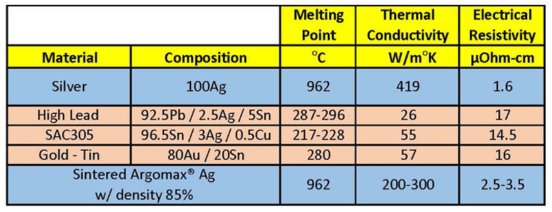
As Chart 1 illustrates, silver is a nearly ideal attachment material, but its melting point makes it prohibitive to use as a reflowed metal. Nonetheless, it has very high thermal conductivity, and exhibits attractively low electrical resistivity. All of these features are superior to solder, including power cycling capability, as will be discussed later.
Chart 1. Die Attach Material Properties
Click image to enlarge
Chart 1 – Die Attach Material Properties
The key to sintered silver is the use of nano particles which fuse at a temperature similar to solder reflow, when aided by modest pressure. Once sintered to a density of ~85%, a thermal conductivity of 200-300 W/mK is achieved. In addition, the interfacial losses are extremely low since the nano Ag also sinters to die and substrate metallization.
One study of note (#2) highlights the significant performance advantage that sintered silver die attach materials can provide for power devices. A comparison was done between a soldered and topside wirebond silicon die pair consisting of an IGBT – Diode (TO247 package) and a similar package and die combination that was constructed using a double sided sintered implementation. The sintered package was capable of switching 200A, compared to the soldered device, which was rated to 130A. Power cycling yielded a 15 X improvement with sintering, and the sintered package was still operational after 150k cycles of 15s on, 15s off with a delta Tj of 100C.
This type of performance and durability can have an immediate impact on existing silicon die implementations as well as setting the stage for the greater use of SiC technology. In addition, sintered silver can support significantly higher die operating temperatures of SiC, since the sintered silver is stable up to the melting point of Ag, which is 962 degrees C.
Another significant advantage of SiC technology is the much smaller die sizes required compared to silicon when switching the same currents.
As the different types of high volume production applications for sintered silver have grown, so have the material types. While the initial sintered silver applications relied on silver nano paste, film as well as preforms have emerged as viable product types, which have enabled new manufacturing processes. Wafer level lamination is now viable with nano silver film. Once the wafer is laminated, the wafer can be diced with standard equipment. An alternative process has also been developed that can laminate individual dies from the wafer and immediately sinter them on a target substrate. This is referred to as the Die Transfer Film process. The advantage of DTF is that only known good die are laminated and sintered, which can provide significant advantages when being used with SiC, which may have yield issues in the start-up phase of new wafer fabrication lines.
Summary
The use of materials such as DBC alumina and DBA alumina and well as double sided cooling enabled with top and bottom substrate are being deployed to advantage in power module designs. In order to realize the full advantages of Silicon Carbide technology, new die attach materials such as sintered silver are being deployed, enabling higher operating temperatures, increased current densities and enabling significantly extended power cycling performance. These advances will yield smaller, lighter, more robust power inverter designs for the new generation of traction inverter products for automotive and other uses.
References:
(1) Double-sided Cooling for High Power IGBT Modules using Flip Chip Technology – C. Gillot; C. Schaeffer; C. Massit; L.Meysenc, 2001 - IEEE Proceedings
(2) Double-sided Sintered IGBT 650V/200A in a TO-247 Package for Extreme Performance and Reliability – C. Greca; P.Salerno; J. Durham; et al. 2016 - 18th Electronics Packaging Technology Conference
Alpha Assembly Solutions