GaN efficiency for chargers and adapters
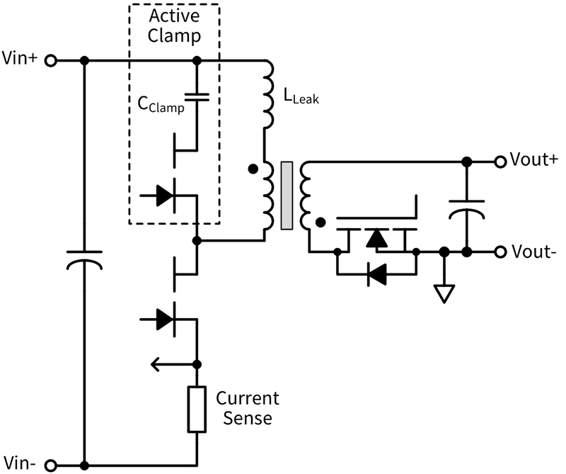
Figure 1. Simplified circuit of the active clamp flyback (ACF) topology
Introduction
It is estimated that 4 billion chargers and adapters are produced globally every year. They charge our mobile phones, tablets, wearables, and the myriad of other consumer electronic goods we consume continuously. The cost of the adapter is undoubtedly a significant consideration for original equipment manufacturers (OEMs), but consumers expect convenience, particularly a very small form-factor and lightweight. Regulatory requirements also play a role but primarily for standby power consumption, not energy efficiency. Efficiency is indirectly mandated by the surface temperature limits for safety. As the chargers become smaller and the power delivered increases, energy efficiency must keep pace to limit the dissipated power to prevent the case temperature from becoming too hot. For today’s small form-factor adapters in the power range up to 65 W, this translates to efficiency in the 92-95 percent range at full power.
For adapters rated 65 W and below, power factor correction (PFC) is not required. Not having to include the PFC circuit is a distinct advantage for this power range because it translates to a simpler, smaller circuit and thus lower cost. Recently, USB PD adapters with one or more outputs are becoming ubiquitous for many of our portable devices. This article addresses what role the power switch plays in improving the adapter’s performance, density, and cost and provides the considerations for applying newer technologies. Traditionally, the power transistors have been silicon-based; however, recent trends clearly show that wide-bandgap transistors, GaN particularly, are becoming the standard for high-performance, small form-factor adapters.
Topology trends
To accommodate universal input voltage worldwide (85-265 VAC), power supplies are commonly split into a boost converter on the front-end for power factor correction, followed by a DC-DC stage to isolate and convert the fixed DC bus voltage to a lower regulated output. But since PFC is not required below 65 W, this stage is replaced with a simple bridge rectifier and bus capacitor. The DC bus voltage directly tracks the input voltage, so it varies over a 3:1 range depending on the line voltage. Thus, the DC-DC stage must now provide not only isolation, voltage scaling, and wide-range load regulation but wide-range line regulation also. Given the 3:1 input range and typical 4:1 output voltage range of USB-C PD, the DC-DC converter at the heart of the adapter has to regulate over a 12:1 combined voltage conversion range. The go-to topology for this function has been the traditional flyback converter and its several variants.
The classic flyback converter operating in discontinuous conduction mode (DCM) can easily handle the wide voltage range, but it is not known for being particularly dense or efficient. The transformer is actually a coupled inductor used to store and transfer energy, and the leakage inductance between primary and secondary also stores energy that must be managed. One method is to use a simple resistor-capacitor-diode (RCD) snubber circuit to dissipate the leakage energy, but this is lossy and reduces efficiency. Resonant and soft-switching techniques add some circuit complexity but can recover the leakage energy while improving switching losses at the same time. One method is the quasi-resonant (QR) approach, also known as “valley-switching.” This topology helps to reduce but not eliminate turn-on losses partially. Because of this, QR flyback converters are rarely operated at more than 65 kHz, and thus the transformer is large compared to topologies operating at hundreds of kHz.
A more popular variant, found in many of the smallest form-factor chargers today, is the active clamp flyback (ACF) converter. In this topology, the clamp transistor turns on when the main switch turns off, providing a current path to recover the energy stored in the leakage inductance. This leakage inductance and the clamp capacitor resonate and transfer energy to the load through the transformer, rather than dissipating it in a snubber; At the end, resulting in improved efficiency. When properly designed, the ACF transistors operate in zero-voltage-switching (ZVS) mode, thus nearly eliminating switching loss and enabling efficient operation at much higher frequencies than conventional or QR flyback. The higher frequency enables smaller transformer structures.
Common in these flyback-based topologies is that the transistors’ voltage rating must be higher than the bus voltage. The resonant topologies use the transistor output capacitance (COSS) as part of the resonant circuit, so a smaller capacitance is key to achieving low loss at higher frequencies as well as reducing the size of the transformer and electromagnetic interference (EMI) filter components.
Considerations for power transistor technology
For many years and even today, silicon (Si) superjunction (SJ) transistors like CoolMOS™ have been the dominant transistor technology used in chargers/adapters. SJ transistors provide low RDS(on), excellent current-handling capability, easy gate drive, and time-proven reliability in a small package, all at a low cost. Given the wide voltage range necessary for adapters, and the overvoltage transients due to leakage inductance and lightning-strike surge transients, even 650 V transistors were often not sufficient, and 700-800 V variants were used for some applications. This is one area where GaN has a significant advantage over Si. Si transistors enter avalanche breakdown when the applied voltage exceeds the rated voltage. Some designs use this “Zener-like” effect as a snubber to clamp overvoltage transients. But even if the energy is within the safe operating area (SOA) of the transistor, this method increases power loss and may result in the generation of additional undesirable EMI. Moreover, the considerable energy from a surge may exceed the avalanche energy capability and destroy the transistor.
GaN transistors, on the other hand, have a voltage rating far below their actual destructive breakdown voltage. The transistor’s rated voltage is based on prescribed application conditions to meet the desired reliability level over the device’s lifetime. For example, for the CoolGaN™ 600 V e-mode HEMT, the destructive breakdown voltage is typically more than 1,000 volts, and it has pulsed voltage ratings of 750 V at various conditions. This is a perfect match for the ACF topology, where the leakage energy is managed with the resonant circuit, and lightning strike surge voltages are accommodated by GaN’s high pulse voltage rating.
The second significant benefit of GaN transistors is that, for a given RDS(on), the output charge is an order of magnitude smaller than a comparable Si transistor. This can be a confusing specification because the capacitance of Si transistors is nonlinear and might look comparable, but when integrated over the full operating voltage, the QOSS for GaN is clearly superior. This is a crucial factor in enabling operation at a higher frequency. During soft-switching transitions, energy stored in the transformer inductance is used to “losslessly” commutate the voltage transition from one transistor to the other. For a given inductor current, the deadtime required for the transition is directly proportional to the transistors’ charge. For example, a 65 W GaN-based ACF converter may need 100 ns for ZVS commutation. Si SJ technology would require 1,000 ns for the same conditions due to its ten times larger QOSS. When operating at 300 kHz, 100 ns is only 3 percent of the total period, but a microsecond is one-third of the entire period!
Deadtime is not productive for transferring power to the secondary-side, so when the deadtime is more than a few percent of the total period, there is a penalty in conduction loss due to increased rms current. The only way for superjunction technology to work at 300 kHz would be to increase the circulating energy stored for commutation significantly, but this correspondingly increases the RMS current and conduction loss. Thus, GaN transistors, with their low QOSS are vital to operating ACF at a higher frequency while maintaining high efficiency.
Gate drive requirements
Gate drive requirements for GaN transistors are different than those for Si. One key difference is that the threshold and fully-on gate-source voltage (VGS) are significantly lower for GaN than for Si transistors. While this can be good news because it reduces gate charge, it can also create challenges in keeping the transistor off when it is supposed to be off. Referring to the ACF circuit in Figure 1, note that the two transistors are configured as a half-bridge, with the main switch on the bottom and the active clamp as the high-side switch. The controller and low-side transistor driver are powered from a bias supply. But the high-side needs a floating power supply for its gate driver. In big telecom or datacenter power supplies, a separate DC-DC converter is afforded to provide this floating bias power for the high-side. But in the adapter/charger segment, the size and cost of this approach are prohibitive.
A common method for powering the high-side is the so-called “bootstrap” power, in which a reservoir capacitor for high-side bias is charged-up through a diode from the low-side bias supply when the low-side is on. When the high-side is on, it draws its bias from the reservoir capacitor, which must be periodically replenished (each time the low-side is on). When the circuit is operating continuously, this is a very effective and low-cost method for powering the high-side. But the challenges are how to operate in discontinuous modes. For example, on first power-up, or similarly after a long time-out period between bursts in standby-mode, the bootstrap capacitor may be discharged, and the high-side driver circuit is therefore un-powered. When the low-side then turns on, the high-side transistor sees a rapid rise in the drain-source voltage (VDS) – and this dV/dt injects current into its gate, pulling it high. Since the high-side gate driver circuit is not yet powered, it may not be capable of keeping the high-side transistor VGS below its turn-on threshold. This causes spurious turn-on and is commonly known as “Miller-induced” CdV/dt turn-on.
Given the half-bridge configuration of the power transistors used in ACF, it is clearly undesirable to have the high-side turn-on at the same time as, and as a result of, the low-side turn-on. Even if the resulting shoot-through current is not destructive (since the clamp capacitor is in series), it can still lead to erratic and unexpected circuit behavior. For example, the shoot-through changes the state of charge of the clamp capacitor, and it creates a current spike in the measurement shunt used by the controller. This can result in control misbehavior because the controller interprets the current spike as transformer current hitting the turnoff threshold.
So how can spurious turn-on of the high-side be avoided when the bootstrap capacitor is not charged? Generic gate driver ICs sometimes include a clamp circuit designed to operate in conditions like this. But traditional approaches intended for Si transistors are dependent on higher threshold voltage, like 3-4 V typical to Si MOSFETs. Accordingly, the circuits begin clamping in the 1-2 V range, and unfortunately, they take hundreds of ns to begin clamping. But GaN transistors can already be conducting a lot of current at these gate voltages. GaN needs clamping to occur at 1 V or lower, and the clamping action has to be as fast as the GaN transistors. Infineon has developed a “fast-clamp” circuit in its existing Si gate driver IC process that can clamp at 0.8 V within 20 ns, even with no supply voltage available to the gate driver IC. This IC process, utilized in Infineon’s EiceDRIVER™ products, is a field-proven industry-standard for datacenter, telecom, and industrial power supply, drive, and inverter applications. The IC platform includes high-speed galvanic isolation rated to withstand common-mode transients’ immunity (CMTI) of 150 kV/µs – among the highest immunity levels available today.
Integrated solution for high performance
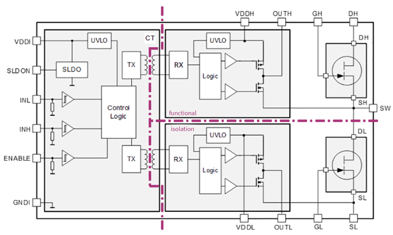
To optimize the performance of the fast-clamp driver combined with GaN transistors, the intervening impedance between them must be minimized. Infineon has taken the approach of integrating both the high- and low-side GaN transistors (190 mΩ), along with the new half-bridge driver into a single iQFN 8x8 mm package – making a half-bridge integrated power stage (IPS), shown in Figure 2.
Click image to enlarge
Click image to enlarge
Figure 2: Block diagram (a) and the iQFN 8x8 mm package (b) of the CoolGaN™ half-bridge IPS
Infineon’s integration and partitioning approach provides several advantages over competitive offerings. First of all, no external digital isolators are required. The propagation delay is short (47 ns), and more importantly, the delay mismatch between the high- and low-side drivers is only a few ns, making it safe and easy to trim deadtime to a minimum for optimal efficiency. The gate drive RC network is external, allowing for tuning the switching speed to balance the losses vs. EMI. The capacitance across the isolation barrier is extraordinarily small, and this reduces common-mode EMI currents. And finally, both the high- and low-side drivers are fully isolated. Even though the low-side typically shares a common ground between the controller, driver, and low-side transistor. This is important because, in the ACF topology, a shunt resistor in the low side source path is often used to sense current, which shifts the effective ground reference point of the low-side GaN driver. If it is not isolated, the shunt voltage subtracts from the applied gate driver voltage, which interferes with proper control of the low-side gate. So, even though complete safety isolation is not required, having isolation on the low-side driver improves performance and simplifies the circuit and PCB layout, eliminating concerns about ground shifts.
High-performance results
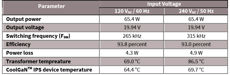
To evaluate the performance of the CoolGaN™ integrated power stage (IPS) 600 V* in an ACF application, a 65 W universal-input converter prototype was designed and built. The synchronously-rectified secondary output is through a USB-C PD interface supporting 5 to 20 V. Table 1 shows the operating conditions and full-power efficiency. Note that the frequency shifts higher by nearly 20 percent from low- to high-line condition. But because of the ZVS operation, the temperature of the CoolGaN™ IPS device changes very little. On the other hand, the transformer core additionally dissipates 0.5 W due to the higher operating frequency. Nevertheless, the overall operating efficiency is ≥ 93 percent over the full range, making this design suitable for small form-factor, hence high-density adapter designs. Additional work is underway to demonstrate another topology variant soon: the hybrid flyback converter, further improving efficiency using the same CoolGaN™ IPS device.
Click image to enlarge
Table 1: Performance of 65 W ACF adapter prototype using CoolGaN™ IPS technology
Summary
Power switch plays a vital role in improving the adapter’s performance, density, and cost. This article presented the technology trends and outlined considerations and requirements for applying newer power transistor technologies. Infineon’s integration and partitioning approach delivers significant advantages over competitive offerings. An ACF application based on the design and implementation of a GaN-based 65 W universal-input converter prototype demonstrates the high-performance results, which open up a new era in power electronics for low-power applications.
Infineon’s CoolGaN™ integrated power stage (IPS) technology is a breakthrough for adapter and charger systems. Thanks to the integration, it enables high power density in a small form-factor and an output power range up to 65W. This advantage, which translates to efficiency in the 92-95 percent range at full power, can be realized by implementing CoolGaN™ IPS in a half-bridge topology allowing for increased switching frequency and reaching higher efficiency at the same time.
To explore Infineon’s full system solutions for USB-PD adapter and mobile charger designs, please visit our USB PD website. To learn more about our GaN solution portfolio, be sure to check out our GaN HEMT page or see the adapter demos at Infineon’s Virtual Power Conference flanking PCIM Europe digital days (May 4-6)) and future conferences.
*The CoolGaN™ IPS 600 V family of products will be available soon. Engineering samples are already available. Contact our support for more information