Tracing SiC FET history and outlining the state of the art for this hybrid of silicon MOSFET and silicon carbide JFET technology
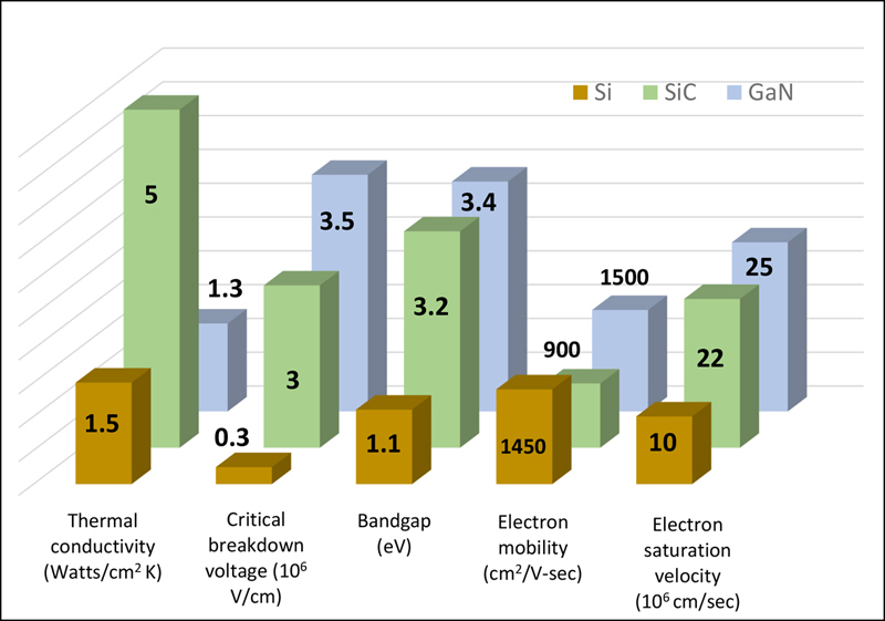
Figure 1: Si, SiC and GaN material characteristics
A basic building block in power conversion electronics is the semiconductor switch. The ideal is one with no static or dynamic losses that can withstand high voltage in the off state and with no leakage when on – but that is always just out of reach. One of the closest though is the wide band-gap technology SiC FET which is allowing significant improvements in efficiency in old and new converter applications.
A little history
Perhaps surprisingly, the first semiconductor ‘device for controlling electric current’ was patented as early as 1925 by JE Lilienfeld, using copper-sulfide, and we would recognize it today as a Field Effect Transistor. Practical manufacturing was not possible then, so it was another twenty-three years before Bardeen, Brattain and Shockley introduced the Bipolar Junction Transistor and the era of semiconductor switching could begin. Early BJTs using germanium were leaky, with limited ratings and poor gain, but silicon devices were a step improvement and initially dominated the market in switching power converters. Indeed, they are still used today at low power, for absolute minimum cost. BJTs do not switch efficiently above a few tens of kHz however, meaning that magnetics have to be relatively large, heavy and expensive.
The MOSFET, introduced in the late ‘70s and early ‘80s, quickly took over with its easy drive and types were soon available with ratings suitable for low and medium power conversion. High power operation was, and still is, limited by device on-resistance as power dissipated is proportional to the square of current. IGBTs however, combined the near-constant saturation voltage of a BJT with the gate drive of a MOSFET, so power increases just proportionally with current. The devices therefore became the default solution for high-power conversion up to the mega-watt range. Despite this, switching losses are significant with IGBTs, often limiting operating frequencies to less than 10kHz in inverters and motor control and again, as with BJTs, associated magnetics are large.
To overcome the magnetics size issue, operation at hundreds of kHz has become possible with the latest ‘super-junction’, low on-resistance MOSFETs, which are competitive with IGBTs to tens of kW. To extend the power and frequency range further though is problematic with silicon, so alternative wide band-gap (WBG) materials Silicon Carbide (SiC) and Gallium Nitride (GaN) were considered. These materials have lower die on-resistance per unit area and high electron saturation electron velocity, for low conduction losses. Because of the high critical breakdown voltage of both SiC and GaN, die can anyway be smaller which produces lower device capacitances and consequent faster switching speed with low dynamic loss. Additionally, SiC has much better thermal conductivity than silicon or GaN so more power can be extracted from a die for a given temperature rise, which is anyway a higher rated maximum with SiC. Figure 1 gives the headline material characteristics of SiC and GaN compared with silicon.
Challenges with WBG devices
While an improvement over silicon, practical WBG devices still have had their historical and on-going challenges. As the main contender, SiC inherently has more lattice defects than silicon, affecting electron mobility and on-resistance. SiC gate threshold voltage shows instability and hysteresis and gate oxide degradation has been seen to occur with stress, such as over voltage and short-circuits. Bulk lattice defects or ‘Basal plane dislocations’ appear to grow and migrate under particular conditions increasing leakage current and on-resistance. The effects have been mitigated by process improvements over the years but manufacturers still have to rely on expensive defect screening during fabrication for acceptably low field failure rates.
Both SiC MOSFETs and GaN HEMT cells additionally have sensitive gate drive requirements, with SiC requiring a high on-state drive voltage for full enhancement, close to the absolute maximum value. GaN has a very low threshold voltage, with a worry about spurious turn-on with transients and again, it is close to its absolute maximum. Reliable circuits therefore need to include careful protection against stress from voltage overshoots or transients. GaN HEMT cells additionally have no avalanche rating, so must be very conservatively rated.
The SiC FET – a step closer to the ideal
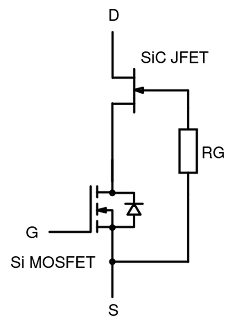
The family of silicon carbide switches includes JFETs which are simpler, have lower losses and, without a gate oxide, are more robust than MOSFETs. They are normally-on however with 0V gate drive so there is a worry that ‘shoot through’ could occur in converter circuits, particularly under transient conditions such as start up and shut down. This has led to the re-invention of the ‘cascode’ concept, or SiC FET, putting a low voltage silicon MOSFET in tandem with the SiC JFET to yield a normally-off device, with loss characteristics dominated by the JFET but with the easy gate drive of a Si-MOSFET. (Figure 2).
Click image to enlarge
Figure 2: The SiC FET schematic
The Si-MOSFET in the SiC FET is specially designed and being low voltage, its zener-protected gate is very robust and can be driven to around 12V for full enhancement, with a large margin of safety away from the absolute maximum of typically +/-20V. The gate threshold voltage is stable and has no significant hysteresis. The cascode arrangement usefully exhibits a reliable avalanche characteristic for overvoltages and a consistent short-circuit withstand rating, independent of gate drive voltage.
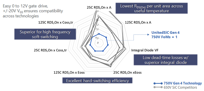
For conduction and dynamic losses, the SiC FET has advantages as well, with an intrinsically better channel electron mobility than a SiC MOSFET, for lower specific on-resistance. Along with shorter channel length, this yields smaller die for the same conduction losses, which in turn means smaller device capacitances and lower dynamic losses. Die size and losses can be traded in fabrication, so to realistically show the advantages of a SiC FET, Figures of Merit (FOMs) are useful. Figure 3 shows some FOMs of SiC MOSFETs normalized to those of a Generation 4 SiC FET from UnitedSiC, all in the same voltage class.
Click image to enlarge
Figure 3: FOMs for a SiC FET compared with SiC MOSFETs
FOM RDS.A, the product of on-resistance and die area is a useful measure as it shows how conduction loss can be traded for die area with a consequence being yield per wafer and cost for the same performance. FOM RDS.EOSS, on-resistance x switching energy, is a measure of total conduction and dynamic losses, other things being equal, particular under ‘hard’ switching operation. RDS.COSS(tr), on-resistance x time-related output capacitance is useful to evaluate devices for high-frequency soft-switched applications. In the figure, values are given at low and high temperatures with the SiC FET better in all cases, for all FOMs. Switching speeds are so fast for the SiC FET that in practical circuits, edges need to be deliberately slowed to avoid high EMI levels and voltage overshoots. Gate resistors are not an ideal way to do this, due to the isolating effect of the Si-MOSFET, but small RC snubbers dissipating minimal power have been shown to be effective.
Third quadrant conduction of SiC FETs is more ideal
In certain power conversion topologies, the switches conduct in reverse’ in the so-called ‘third quadrant’, such as motor drives or hard switched types with inductive loads. IGBTs need a parallel diode, but Si- and SiC MOSFETs and GaN HEMT cells will conduct in reverse through their channels. The two MOSFET types however have a parasitic body diode that conducts during any ‘dead time’ before the channel is active and this stores charge which has to be recovered in the switching cycle, leading to a spike of dissipation. The SiC MOSFET body diode also has a forward drop of around 4V which contributes to power loss. The GaN cell has no parasitic body diode, so no appreciable reverse recovery charge but when conducting through its channel by ‘commutation’ in the dead time, its voltage drop is the sum of the gate threshold and any negative off-drive, which can total to several volts, again causing dissipation.
The SiC FET in contrast has a body diode effect dominated by the low voltage Si-MOSFET which has very low reverse recovery charge, about a third of a SiC-MOSFET and about a hundred times less than an otherwise similar high voltage Si-MOSFET. The forward voltage drop of the SiC FET is also lower at about 1.5V. The reverse recovery waveforms of a UnitedSiC SiC FET and a current super-junction MOSFET in the 400V class are compared in Figure 4.

Click image to enlarge
Figure 4: A SiC FET compared with a SJ Si-MOSFET showing around 100x less recovered charge
The relatively poor QRR performance of SJ Si-MOSFETs has precluded their use in some topologies such as the bridgeless ‘Totem Pole’ power factor correction stage, operating in continuous conduction mode. SiC FETs are however perfectly suited.
SiC FET reliability is assured
Despite the decades-long pedigree of cascodes, versions using SiC technology may seem new and require proof of reliability. Field and lab data demonstrates this, but additionally, the identified issues of SiC gate oxide degradation are inherently not present and the low-voltage Si-MOSFET gate is robust with a thick oxide, proven to be reliable. Strong avalanche and short circuit withstand ratings contribute to reliability performance that allows UnitedSiC to routinely achieve automotive AEC-Q101 qualification for their parts. The company also uses silver-sintering for die attach in its latest products for its 6x better thermal conductivity than solder. This keeps junction temperature rise low and reliability high.
SiC FET evolution continues
UnitedSiC now manufactures 4th generation SiC FETs with increased voltage ratings, best-ever FOMs and on-resistances so low that the substrate itself has become a limit, so wafer-thinning techniques are employed for even further gains. Package options have been expanded from the original TO-247 with side-by-side die to ‘stacked’ arrangements with Kelvin source connections and leadless DFN8x8 versions for MHz switching, with their low lead inductance. Further developments include more package options and parts with uncommitted JFET gate connections for the ultimate in switching speed control.
SiC FETs – the better solution
We will never actually achieve the perfect switch but SiC FETs are pretty close, with a performance/price ratio that is increasingly attractive. Device voltage ratings are available to 1700V, and on-resistances can be sub-5-milliohm depending on voltage class. To see the range and as a design aid, UnitedSiC have made their ‘FET-Jet’ web-based simulation tool available which predicts the loss and stress level performance of their devices in a range of AC-DC, DC-DC, isolated and non-isolated application circuits.