The Power and Evolution of GaN – Part 5
Part 5 of a 6 part series
In this series, how the superior switching speed of gallium nitride (GaN)-on-silicon low voltage power devices have enabled many new applications is being discussed. These new applications are transforming industries such as light detection and ranging (lidar) for autonomous vehicles, envelope tracking for 4G and 5G communications and large surface area wireless power for the home and office.
In addition to contributing to the performance of these new applications, the growth of GaN devices has led to the development of a strong supply chain, reduction in production costs (through higher yields and higher volumes), and an enviable reliability record. All of this fundamental work with GaN provides adequate incentive for the more conservative design engineers creating power system designs in more mainstream applications, such as DC–DC conversion, AC/DC conversion, and automotive electrical distribution to start their evaluation process. As an example of the contribution to performance GaN devices can make to one of these mainstream applications, a traditional silicon application, the 12 V – 1 V point-of-load (POL) DC/DC converter will be examined.
Meeting the Demands of Power-Hungry Mobile Computing
Consumers want their mobile devices to perform ever-growing array of power-hungry tasks. These performance demands, coupled with the conflicting desire for small, lightweight form factors and extended battery life, translate into ever-increasing demands on the power distribution system. In other words, high-performance point of load (POL) DC-DC converters (the power engines) need to be designed to be small sized while being highly efficient.

Click image to enlarge
Figure 1: POL requirements of mobile products provide perfect platforms for the high performance, extremely small size, and low cost of GaN devices
Reducing the size and decreasing the power consumption of the core power electronics is critical to keeping pace with these demands. Increasing the switching frequency of power transistors is a known path to size reduction. GaN-based power devices, available today, help eliminate the barriers to achieving higher converter frequencies and will drive the next generation of mobile computing.
Increase Speed Without Sacrificing Converter Efficiency...Through Integration
Increasing frequency is a proven method to reduce size. Equally important for mobile systems is to achieve a high efficiency solution, a key to saving battery life. Converter efficiency can be significantly improved with single-chip integration such as that provided with eGaN FETs and ICs.
A key speed bump on the road to high frequency and efficiency is parasitic inductance. Parasitic inductance has been demonstrated to reduce switching speeds [1] and therefore increase system power losses. By integrating two eGaN power transistors into a single device, interconnect inductances and the interstitial spacing needed on the PCB are greatly reduced or even eliminated.
Click image to enlarge
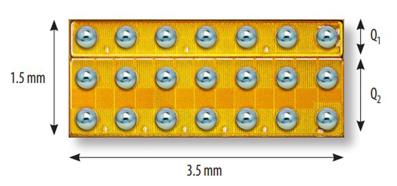
Figure 2: EPC2111 30V monolithic half-bridge with on-resistance 19 m ohm (Q1) and 8 m ohm (Q2)
A second advantage of integration is the ability to optimize die size and the shape of both the control FET and the synchronous rectifier. Integration allows for the reduction in size of the control FET (Q1) to reduce the switching related losses and a larger synchronous rectifier (Q2) to reduce conduction losses. It also allows for the creation of control FETs that are “long and thin” (see Figure 2) which serves to reduce the power loop inductance. The EPC2111 (Figure 2) is a monolithic eGaN half-bridge IC designed for high step-down point-of-load converters where the control FET (Q1) is approximately one fourth the size of the synchronous rectifier (Q2). Each FET is capable of carrying a continuous current of 16 A in a tiny 5.25 mm2 footprint. The EPC2111 is nearly one seventh the footprint area of comparable Si MOSFETs and can switch much faster and has lower parasitic capacitances than equivalent silicon devices. The result is the lowest switching loss operation even at very high switching frequency (10 MHz), making this GaN device ideal for POL applications.
1000 W/in3 Power Module – EPC9204 DrGaNPLUS
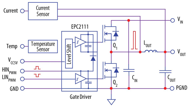
The smallest, most cost effective and highest efficiency non-isolated 12 V to 1.0 V POL converter, suitable for high-performance computing, cryptocurrency and telecommunication applications, can be achieved by employing monolithic eGaN® IC half bridges such as the EPC2111.
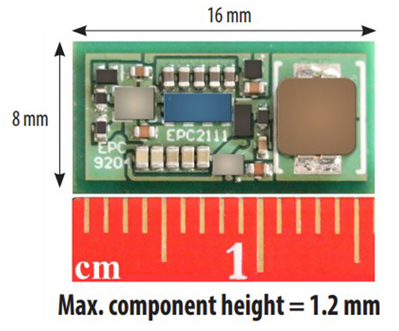
An application demonstration using the EPC2111 is the EPC9204 DrGaNPLUS module (shown in figure 3). It is a synchronous buck converter yielded a power density of 1000 W/in3 and is capable of delivering 12 A.
Click image to enlarge
Figure 3: EPC9204 development board boasts a power density of 1000 W /in3 based on component height only and when operating at 12V input, 1V at 12A load
The EPC9204 power module, with the block diagram shown in figure 4, is configured as a synchronous buck topology using the EPC2111 eGaN monolithic half bridge. The EPC9204 power module, shown in figure 3, also features the PE29102 half-bridge gate driver IC from pSemi Corp., input and output filters, as well as current and temperature sensing. The tallest component on the EPC9204 board is a mere 1.2 mm. The high frequency capability of eGaN FETs greatly reduces the filtering requirements, allowing for an optimized output filter inductor with much smaller size and lower loss.
Click image to enlarge
Figure 4: Block diagram schematic of the EPC9204 development board fitted with EPC2111, is ideal for 12 V to 1 V POL conversion
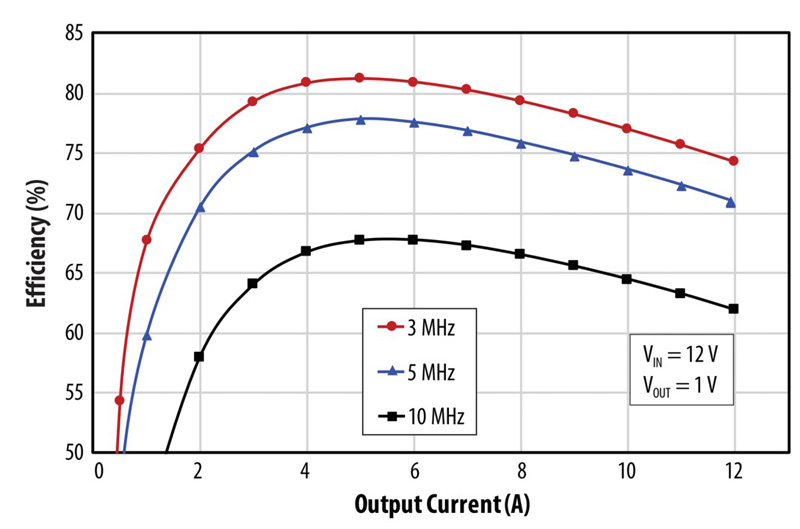
The EPC9204 achieves a peak efficiency of 78% at 5 A load and 5 MHz, with a maximum FET temperature of 100⁰C under 400 LFM airflow. Figure 5 shows a plot of the load current range efficiency up to 12 A load when operating at 3, 5 and 10 MHz respectively.
Click image to enlarge
Figure 5: EPC9204 efficiency vs. output current for 12 VIN to 1 VOUT using EPC2111 eGaN IC Monolithic Half-Bridge
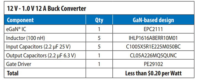
Migrating a high frequency 12 V to 1 V POL converter design from silicon MOSFETs to eGaN ICs is an obvious choice, due to higher efficiency, and also the reduction in both size and cost. Table 1 shows a bill of materials for a converter that yields a cost per watt of less than $0.20.
Click image to enlarge
Table 1: Bill of Materials for monolithic eGaN 12V to 1V converter based on 500 k unit pricing
The eGaN IC based 12 V to 1 V, 12 A load converter yields a peak efficiency of 78% at 5 MHz with a power density of at least 1000 W/in3, all with a cost below $0.20 per watt.
Summary
Consumers continue to demand that mobile devices perform an ever-growing array of power-hungry tasks while remaining small and lightweight. Reducing the size and decreasing the power consumption of the core power electronics is critical to keep pace with these demands.
The power conversion circuits in these power systems in mobile devices occupy nearly half the space and defines the maximum height of the motherboard. The most straightforward way to achieve a size reduction is to increase switching frequency, enabling a reduction in the size of the output capacitance and inductance. Silicon-based POL systems typically operate at 1 MHz and below. The ability of GaN-based power devices to operate efficiently at high frequency, such as 10 MHz, will drive significant reductions in board area and height for next generation mobile computing.