Part 6 of a 6 part series
Slightly more than forty years ago, the silicon power MOSFET was a disruptive technology that displaced the bipolar transistor as the power conversion device of choice for the semiconductor industry – and a $12B market emerged.
Click image to enlarge
GaN Cube
The dynamics of this transition taught us that there are four key factors controlling the adoption rate of a new power conversion technology:
- Does it enable significant new applications?
- Is it easy to use?
- Is it VERY cost effective to the user?
- Is it reliable?
In the first article of this serieswe explored how gallium nitride (GaN) technology is addressing each of these factors. GaN has met the requirements to displace silicon solutions: it enables new applications, and these new applications have helped to develop a robust ecosystem, lowered production costs, and created an enviable reliability record.
Since commercial availability of GaN power devices began in 2010, the technology has quickly assumed the position as the presumptive replacement for the aging power MOSFET. The initial adopters came from new markets, such as light detection and ranging(lidar), envelope tracking, and wireless power, that took advantage of the superior switching speed of GaN. These new applications helped develop a strong supply chain, low production costs, and an enviable reliability record. All of these attributes provided adequate incentive for the more conservative design engineers in applications, such as dc–dc converters, ac–dc converters, and automotiveto start their evaluation of GaN. This shift in understanding of the benefits of GaN technology is leading to a rapidly increasing adoption rate for gallium nitride power devices.

Click image to enlarge
LIDAR Car
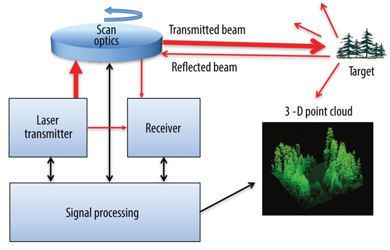
As this series continued, the emergence of GaN in just a few of the many high-volume applications taking advantage of the technology to achieve new levels of end-product differentiation were discussed. One such applicationis the emerging market of lidar, where an ultra-fast high-power GaN-based laser driver is employed. These lidar systems are used in applications such as autonomous cars, drones, and robots as well as home and industrial security systems. The superior performance of GaN power transistors enable groundbreaking laser driver performance. The ability to generate single digit, nanosecond, high-current pulses to deliver hundreds of watts from a few square millimeters is truly remarkable. It is one of the main factors in making affordable, high-performance lidar possible in a small form factor thus fueling the lidar revolution.
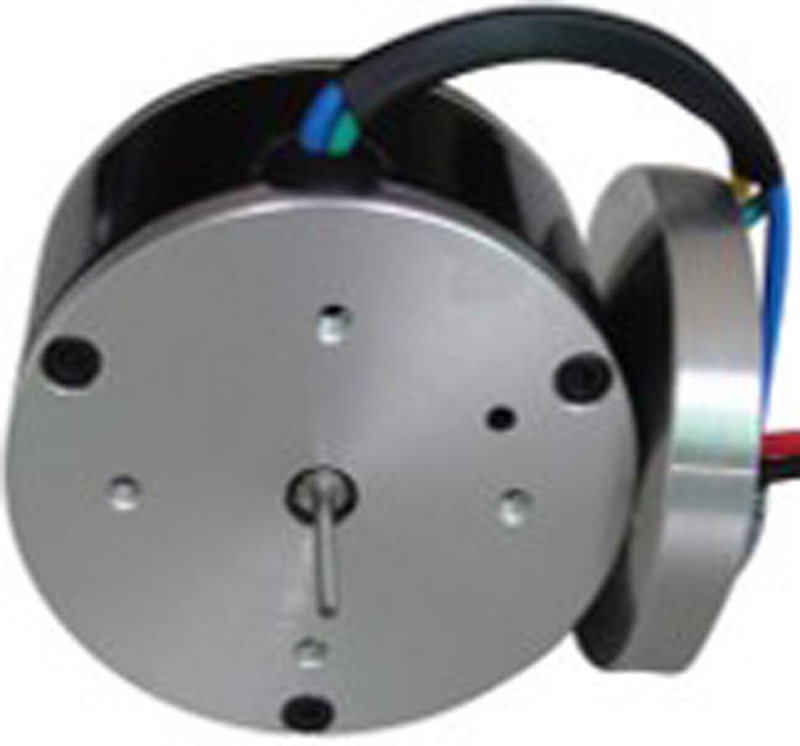
Further in the series, how GaN is transforming medicine by bringing precision control to robotic-assisted surgery was examined. Surgeon directed robots improve surgical precision capability and, in many cases, require minimal invasive access to the patient. Robotic surgery involves control of multiple compact surgical arms using the ultra-reliable, high-performance brushless (BLDC) class of motor drive systems. These surgical systems require a motor with high efficiency, minimal vibration, and precision control. eGaN FETs and ICs offer higher efficiency and precision motor control in a smaller solution than equivalent, traditional MOSFET solutions and are ideal for this application.
There were two articles in the series that addressed the more traditional MOSFET application of DC/DC conversion. In one of these articles, a low cost, high efficiency 12 V – 1 V Point-of-Load (POL)converter design was presented demonstrating how a GaN-based power module, configured as a synchronous buck converter, can yield a power density of 1000 W/in3 capable of delivering 12 A per phase. This high level of power density is ideal for high-performance computing, cryptocurrency mining, and telecommunication applications.
In the second of these articles, how to build the smallest and most efficient 48 V to 5 - 12 Vconverter was shown. The eGaN-based power module, configured as a synchronous buck converter, yielded a power density of 1400 W/in3 when operating at 48 V input, 12 V output and a 10 A load. This design is capable of producing an output voltage ranging from 5 V to 12 V and delivering 14 A per phase of output current making it ideal for high density computing and telecommunication applications.

Click image to enlarge
48V GaN
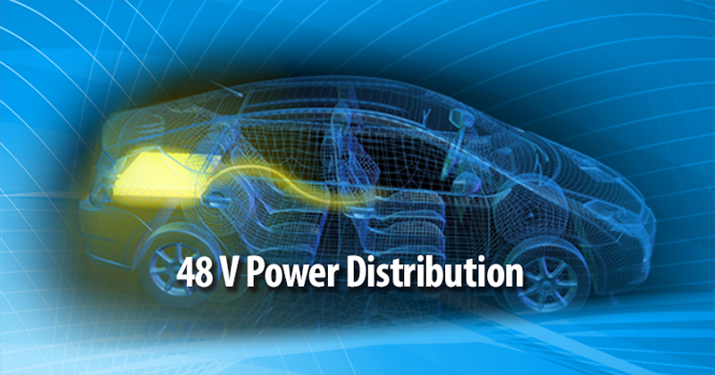
There are very significant performance advantages gained from GaN in 48 VIN conversion and this is a market where growth is exploding for multiple reasons. The first is the increased demand in applications such as Artificial Intelligence (AI), gaming, cloud computing, and autonomous cars for higher computational density. These applications are leading the migration from 12 V to 48 V systems. The second is the migration of automotive systemsmoving from 12 V distribution systems to 48 V systems. This change is driven by the increase of power hungry electronically-driven functions and the emergence of autonomous vehicles creating additional demands from systems such as lidar, radar, camera, and ultrasonic sensors upon the power distribution system. In all topologies with 48 VIN, the highest efficiency is achieved with GaN devices due to their lower capacitance and smaller size than that of equivalent silicon devices. With recent pricing declines in GaN power transistors, the cost comparison with silicon-based converters now strongly favors GaN in all of these leading-edge solutions.
As the adoption rate of GaN explodes, it is important to remember that, while GaN has made many advancements in just a few short years, it is still far from its theoretical performance limitations and thus there are profound improvements that can continue to be achieved. The greatest opportunity, however, for GaN to impact the performance of power conversion systems comes from the intrinsic ability to integrate both power-level and signal-level devices on the same substrate.
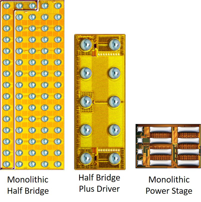
Click image to enlarge
ICs
The first commercial GaN ICs appeared in 2014 in the form of monolithic half-bridge devices. As the technology progressed, more complex integration started to appear in the market, such as the EPC2115. This product includes two power transistors and driver circuitry that enables efficient operation up to 7 MHz when driven by a low power logic gate. In March 2019 the introduction of a monolithic half bridge that incorporates driver and level shift circuitry to create a monolithic power stage is planned. This IC will be followed by full system-on-a-chip power devices that will ultimately obsolete discrete transistors in power conversion applications.
In time, the performance and cost advantages of GaN-on-silicon will result in a majority of applications currently using silicon-based devices converting to the smaller, faster, cheaper, and more reliable GaN technology.