The SiC Evolution and GaN Revolution for Electric Vehicles
While SiC will likely remain the preferred technology at high voltages, at lower voltages EVs can employ GaN devices for better power density and efficiency
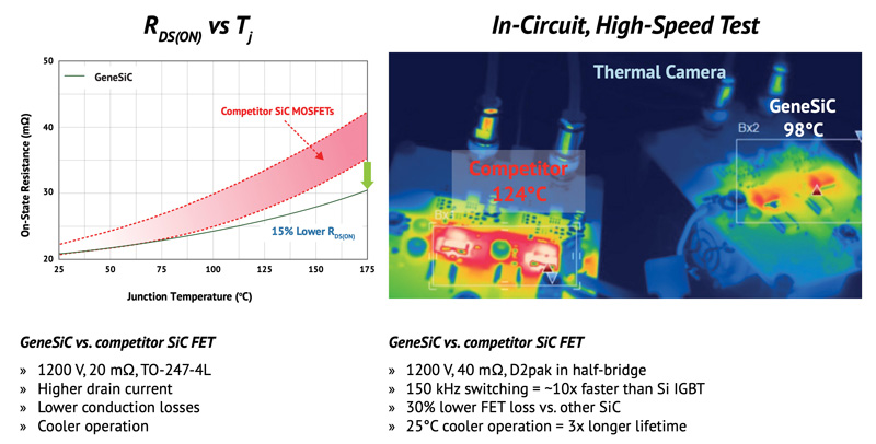
Figure 1: Enhanced temperature stability ensures consistent efficiency under all conditions
Governments worldwide, seeking to meet climate-change pledges, are driving the transition to electric vehicles through legislation and financial inducements. According to Fortune Business Insights, the total global market for battery and hybrid electric vehicles will grow from $500 billion in 2023 to almost $1,600 billion by 2030, exhibiting CAGR of 17.8%.
Wide-bandgap power technology is a part of the success story, helping accelerate the worldwide adoption of EVs by enabling vehicles to go further between charging. The majority of electric vehicles sold today can travel between 150 and 300 miles between charging. The phenomenon of range anxiety – long seen as a barrier to EV acceptance - is subsiding as more and more potential buyers are able to identify affordable models that fulfil their typical usage requirements. Longer range alleviates the threat of a dead battery at the roadside, or of extended wait times at charging points, waiting for a charger to come free and then to charge the battery.
Silicon carbide has led the infusion of wide-bandgap technology into the EV scene, replacing legacy silicon MOSFETs or IGBTs in the traction inverter, especially. SiC MOSFETs are known for their superior conductivity and switching performance compared to silicon devices. Additional advantages include greater ability to withstand elevated temperatures and high breakdown voltage in relation to device size, which permit enhanced ruggedness and power density.
In other systems mounted on the vehicle, such as the on-board charger and the many DC/DC converters that power the diverse loads throughout the vehicle, gallium nitride high electron mobility transistors (HEMTs) are now coming into the picture. While SiC devices have the upper hand in high-voltage applications, such as equipment connected to an 800 V bus in some high-end vehicles, GaN offers valuable advantages when applied to platforms operating with lower battery voltages up to about 400 V.
Fast SiC for Next-Generation Automotive
SiC is the most commercially mature among current wide-bandgap technologies for power semiconductors. Navitas and other leading manufacturers have released several generations of SiC power MOSFETs, with each successive generation offering increased performance. While realizing a step change in the typical figures of merit achieved with silicon, the new SiC technology encounters its own barriers to further progress. Development typically focuses either on planar technology, which allows limited scope to improve switching performance and RDS(ON) vs. die area, or trench architecture. Here, inconsistencies in the fabrication process tend to cause lower yield leading to higher device cost.
Trench-assisted planar-gate technology has overcome these issues, permitting high-yield manufacturing, fast and cool operation, and extended, long-life reliability. Navitas’ “Gen-3 Fast” (G3F) MOSFETs, which utilize this technology, achieve the industry’s lowest RDS(ON) at high temperatures (figure 1) and lowest energy losses at high speeds.
Both the stable temperature characteristic and efficiency at high speed are valuable attributes in automotive applications, which can be exposed to high ambient temperatures while device power cycling further elevates the junction temperature. Lower energy losses at high speeds enhances scope to increase the MOSFET switching frequency in converter circuits operating at frequencies from 300-800 kHz, permitting the use of smaller passive and wound components to maximize power density within compact module dimensions.
Roadside and On-Board Charging
Compared to level 1 charging at 0.8-1.3 kW/hr and level 2 at 3.3-19.2 kW/hr, DC fast charging at up to 350kW/hr has now arrived and cuts the turnaround time to a few minutes. Using these chargers, vehicles such as large SUVs, which can have battery capacity of about 100 kWh, can now recharge from 10% to 80% in under 20 minutes. To help realize DC fast charging in roadside equipment of acceptable size, new architectures have increased the working bus voltage up to 1,250 V. This requires power devices with up to 3,300 V capability, to cover all main and auxiliary power applications, currently best served by SiC devices such as Navitas’ G3F series.
As far as systems on-board the vehicle are concerned, the position is somewhat different. The on-board charger (OBC) that converts AC power from the charger to a high DC voltage at, say, 400 V or 800 V depending on the vehicle’s battery voltage can range from 6.6 kW to 22 kW. While 800 V battery systems require the safety margin provided by 1,200 V SiC MOSFETs and diodes, GaN-based devices at 650/700 V can be considered for OBCs, DC-DC and traction inverters used in 400 V battery systems.
The bi-directional OBC is a key development in the adoption of EVs within future sustainable smart electrical grid infrastructures. This allows the EV to act as an energy reservoir or as an energy source for other loads, to help manage supply and demand variations and help stabilize the grid. GaN and SiC devices enable advanced, bi-directional topologies and can shrink and consolidate power converters.
Figure 2 illustrates a design for a 6.6 kW OBC and combined 3 kW DC-DC converter in a 210 x 192 x 60 mm enclosure that is smaller, more lightweight, and more efficient than similar designs built using silicon devices.
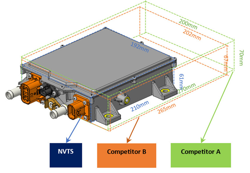
Click image to enlarge
Figure 2: Lightweight, high-power density OBC/DC-DC combination module
DC-DC Converters
Away from the high-voltage, high-power traction and charging circuits, many automotive applications operate from the typical 12 V automotive voltage rail. These include navigation systems, Lidar, seat motors, windshield wipers, and others.
When designing DC-DC converters for these applications, 650/700 V GaN devices can save up to 20% of energy and also significantly reduce circuit size and weight compared to ordinary silicon MOSFETs. However, enhancement-mode (normally-off) GaN FETs have a relatively fragile gate that requires precise control to keep the gate-source voltage (VGS) within the maximum range of -10 to +7 V. The typical threshold voltage is 1-2 V. High-power bridge circuits can expose discrete GaN FETs to potentially damaging negative VGS spikes at low-side turn-off.
GaN ICs meet Automotive Needs
GaN ICs that integrate an optimized gate driver in the same package as the GaN FET can ensure proper control of the VGS to prevent the gate from becoming damaged. Navitas GaNSafe devices integrate the driver and also implement advanced algorithms for dead-time control to prevent shoot-through currents and, with zero gate-source loop inductance, enable switching at frequencies up to 2 MHz to maximize application power density. There are several built-in safety features including high-speed autonomous short-circuit protection that acts within 50 ns and electrostatic discharge (ESD) protection up to 2 kV. ESD protection is typically not provided with discrete GaN transistors.
Unlike conventional multi-chip modules, GaNSafe ICs utilize TOLL and TOLT (TO-Leaded top-side cooling) packages that deliver superior thermal performance and reliability. The TOLT has high current capability and a low profile, similar to the TOLL, and exposes the drain at the surface of the package to enhance heat dissipation and simplify thermal management.
By addressing high-voltage, high-power applications, these devices bring the proven speed advantage of GaN to the automotive world, enabling smaller, lighter modules that contribute to space savings and greater energy efficiency.
Conclusion
SiC wide-bandgap technology has taken a lead role in enabling EVs and charging infrastructure to deliver extended driving range and shorter charging times. Both improvements are needed to convince more car buyers to make the change to electric.
Growing markets bring increased consumer pressure, requiring EV brands and makers of subsystems including the OBC and DC-DC converters used throughout the vehicle to continue striving for increased efficiency, power density, and reliability. GaN ICs that combine 650/700 V power transistors with optimized gate control can now offer a solution that meets these demands. Tomorrow’s EVs will fulfil ever-rising market expectations using a combination of GaN and SiC technologies, chosen for their respective strengths in different roles within the vehicle.