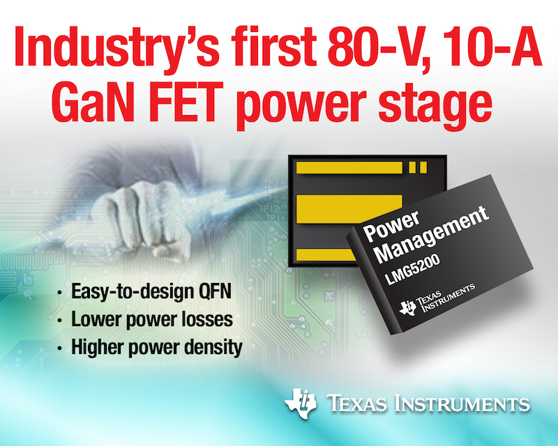
Texas Instruments introduced the industry’s first 80-V, 10-A integrated gallium nitride (GaN) field-effect transistor (FET) power-stage prototype, which consists of a high-frequency driver and two GaN FETs in a half-bridge configuration – all in an easy-to-design quad flat no-leads (QFN) package.
The new LMG5200 GaN FET power stage will help accelerate market adoption of next-generation GaN power-conversion solutions that provide increased power density and efficiency in space-constrained, high-frequency industrial and telecom applications. The power stage will be highlighted as part of a 48-V digital power demonstration at the Applied Power Electronics Conference (APEC), in Charlotte, North Carolina, March 16-18 (booth No. 1001). Follow TI at www.ti.com/APEC15.
“One of the biggest barriers to GaN-based power design has been the uncertainties around driving GaN FETs and the resulting parasitics due to packaging and design layout,” said Steve Lambouses, vice president of TI’s High-Voltage Power Solutions business. “We help power designers realize the full power potential of GaN technology by offering them a complete, reliable power-conversion ecosystem of optimized integrated modules, drivers and high-frequency controllers in advanced, easy-to-design packaging.”
Enabling the GaN advantage
Typically, designers who use GaN FETs that switch at high frequencies must be careful with board layout to avoid ringing and electromagnetic interference (EMI). TI’s LMG5200 dual 80-V power stage prototype significantly eases this issue while increasing power-stage efficiency by reducing packaging parasitic inductances in the critical gate-drive loop. The LMG5200 features advanced multichip packaging technology and is optimized to support power-conversion topologies with frequencies up to 5 MHz.
The easy-to-use 6-mm by 8-mm QFN package requires no underfill, which significantly simplifies manufacturing. The reduced footprint solidifies the value of GaN technology and will help increase adoption of GaN power designs in many new applications, ranging from new high-frequency wireless charging applications to 48-V telecom and industrial designs. For more information on , visit: www.ti.com/gan-pr.
Key features and benefits of the LMG5200:
• Highest power density. The first integrated 80-V half-bridge GaN power stage delivers 25 percent lower power losses compared to silicon-based designs, enabling single-stage conversion.
• Comprehensive GaN-specific quality program for reliability. Read more here.
• Lowest packaging parasitic inductance in the critical gate-drive loop increases power-stage efficiency and enhances dV/dt immunity while reducing EMI.
• Simplified layout and manufacturability. Easy-to-use QFN package eliminates the need for underfill to address high-voltage spacing concerns, improving board manufacturability and reducing cost.
Tools and software
In addition to ordering the available LMG5200 evaluation module (EVM), designers can get started faster using PSpice and TINA-TI models for the LMG5200 to simulate the performance and switching frequency advantages of this technology.
Availability and pricing
Prototype samples of the GaN power stage are available to purchase now in the TI Store. The LMG5200 is priced at US$50 each with a maximum purchase of 10 units. The LMG5200 EVM is available for US$299.